It seems that the article was incomplete, because I still have difficulty imagining how it can be put into practice at home, starting with making a die.
A lot of work was spent, but nothing worthwhile came of it. The configuration of the die must be complex, the working surface must be polished, the workpiece for it must be hardened, and most importantly, the width of the strip must be maintained with fairly high accuracy. Cutting the resulting tube is another task, and riveting it is also quite difficult.
Contents
- 1 Idea
- 2 Tool
- 3 Implementation
- 4 Total
Recently I needed to make a double-sided printed circuit board.
And not just double-sided, but always with transitions between layers, since when soldering there will be no access to the opposite side. And not just with transitions, but with fairly powerful transitions, because relatively large currents are supposed to flow through these transitions. The first thought was to make additional platforms and connect the layers with copper rivets from a suitable wire, but the subconscious protested - the solution was clumsy...
Blog UMNIKA
Start here.
Metallization of holes.
This will probably be the most interesting thing, since the technique I used is rare, and in general, metallization of holes in a printed circuit board is something that still does not have a convenient home technology.
I metallize the holes using brass bushings specially designed for this purpose.
I bought these bushings in Greece (apparently because everything is there), but not in person, but through Ebay. In general, the thing seems to be necessary and useful, but few people sell it.
Here is the link to the seller. And then on to the bushings themselves.
I also found links to people who sell similar bushings, but I didn’t buy from them, I don’t know.
Link 1.
Link 2.
Link 3.
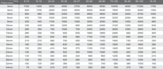
The bushings come in different sizes, I use two of them: the main one - running - outer diameter 1 mm, internal 0.8 mm (the leads of resistors, capacitors and DIP microcircuits pass into the resulting holes) and for thick leads - outer 1.4 mm, internal 1.2 mm (for power transistors, terminal blocks, etc.)
Now the process itself is not complicated, but due to the small size of the bushings, it is painstaking.
The bushings are small, here next to my finger:
Bushings in bags:
To install, you need a pin (a medical needle for injection is also convenient, but this time I didn’t have it on hand) and a punch for flaring.
The punch was turned on a lathe - the tip is 3 mm in diameter, on it there is a protrusion with a diameter of 0.8 mm, a height of 1 mm:
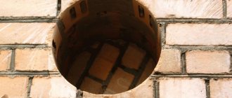
I insert the bushings only where the conductor approaches the platform from above. To save bushings, they do not need to be placed where the vias are located; they can be soldered with a piece of wire. You also don’t have to place it where you can unsolder the part output from the top side of the board (where the parts are). Thus, bushings are absolutely needed where a conductor approaches the pad on the upper side and where the part covers this pad - these are usually electrolytic capacitors, terminal blocks, panels for microcircuits. Here everyone saves at their own discretion (bushings are not as cheap as they would like). In this case, I placed them wherever there are conductors from above; let’s consider this an attack of perfectionism.
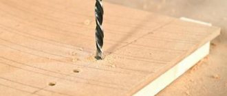
Initially, the holes in the board are drilled by default 0.8 mm (for the main parts). Where I need to put a bushing, I need to drill a hole to the diameter of the bushing (this is 1 mm for the main bushings and 1.4 mm for large ones).
I drill it out on a drilling machine. The diameter of the hole must be maintained quite accurately; if you drill with a 1.05 mm drill, the bushings do not hold in such a hole and fall out when we need to turn the board over to flare the bushings.
So, the necessary holes are drilled, we begin to insert the bushings. It’s not possible to insert a separate sleeve, so we put it on a pin, or it’s more convenient to put on several pieces at once:
And we put it in.
They are inserted tightly and the force on the pin is not always enough to insert it all the way:
Then we press them into the board by hand using a punch so that the head of the sleeve is flush with the board.
Now we turn the board over and flare the bushings on the reverse side using a punch. I do this by securing the punch in a drilling machine, we don’t turn on the rotation, we just use it as a press.
Here's the result:
With some skill, everything turns out quickly and efficiently.
When flaring, the board itself is placed not on a piece of wood (as when drilling), but directly on the steel table of the drilling machine. The bushing head
becomes flat:
Well, that’s all, the vias are metallized!
Continuation
↑ Idea
The idea came unexpectedly. I use crimp lugs for stranded installation wire regularly in my work,
but somehow I didn’t associate them with rivets, until the insulator fell off at one tip...
This is where everything fell into place. At the first moment, all kinds of flaring with a shaped working part began to come to mind, highly desirable, made of hardened steel, with a polished surface. But, in the end, I decided not to bother and work with the tools at hand.
Copper hypophosphite (activator solution)
Diamincopper hypophosphite dihydrate two
Solution: Calcium hypophosphite (calcium hypophosphate) - 20 g. [Ca(PH2O2)2] Copper sulfate (Copper 2 sulfate 5 water) - 25 g. [CuSO4 5H2O] (by the way, sold in gardening stores) Ammonia (pharmacy 10%), = 10% aqueous solution of ammonium hydroxide - 50 ml. (NH3+H20) Distilled water 100 ml. Detergent “Drop” - 3 g. (water, surfactant, sodium chloride, preservative, perfume composition, citric acid, SI 19140, 42090)
1. Copper sulfate 25g + water 50ml = long (+ sediment) 2. Calcium hypophosphite 15g + water 50ml = long 3. 1 pour into 2. (mix) = + sediment 4. filter (discard sediment) 5. + 50 ml. pharmaceutical 10% ammonia 6. + 5 grams of calcium hypophosphite 7. + detergent (liquid soap) - 3 grams
We clean the board with an abrasive detergent without fanaticism, and wash it thoroughly.
At the end of the washing, the water should “stick” to the workpiece, flowing off it extremely reluctantly.
Shake it thoroughly, lower it horizontally into the activator, without touching the bottom.
Remove it horizontally to the surface several times for 2-3 seconds.
The liquid should flow evenly into all holes
We tilt it and touch the edge of the container so that the excess activator flows back (without fanaticism).
Close the container with the activator and tilt it at different angles, trying to allow the activator to spread as evenly as possible.
Then we put it in the oven, set it to 125C and keep it for 12-15 minutes.
Then 175C and hold for 7-8 minutes, open the door and let it cool down to 100C.
We can easily wash it with a non-abrasive detergent and a soft sponge (without water yet).
Use a washcloth to push the detergent through all the holes, calmly and slowly, trying not to miss anything.
Next, use a stream of water to rinse all the holes. no need to wash every single stain.
The activator can be stored for a long time, the main thing is that the ammonia does not evaporate from it, that is, we store it hermetically (in the dark). This means the container is better - a bottle with a minimum of space not occupied by liquid. I kept it on the balcony for a month and it reached -10C. I used it 10 times without problems (the properties of the activator were preserved).
The activator is stable and can be stored for a long time. During use, you need to ensure that there is always a sediment of calcium hypophosphite at the bottom and, if necessary, add a couple of grams. If this is not done, unplated holes may appear.
↑ Tool
Wire cutters, pliers, hole punch and hammer.
A cone awl is an important tool in this matter. I had a drill sharpened in time immemorial (now I can’t even imagine why) - it just fit. Well, and most importantly, a multifunctional tool, commonly called a “tin can,” which plays the role of an anvil. Experiments have shown that the result is quite functional, not factory-made, of course, but this does not matter - the uneven edges of the rivets are hidden under the solder.
Graphitization
Another easy-to-use metallization method. The difference is that for the initial processing of holes, instead of silvering, graphitization is done. Most often, amateurs use store-bought aerosol CRAMOLIN “GRAPHITE” . It is enough to press the finely dispersed fractions of graphite deposited on the surface into the prepared holes. This is easy to do with a small spatula or scraper. There is no need to explain how to make them yourself.
To remove excess, while the paste is still wet, shake the board. Fractions adhering to its surface are washed off with a solvent or removed with fine (grinding) sandpaper. All that remains is to clean the hole with a thin needle.
As a result, it produces the thinnest conductive layer. This method of removing paste has a disadvantage - not all fractions are removed from the hole, which reduces its diameter. A better result is achieved by the blowing method. At home, you can use a vacuum cleaner.
The described methods for metallizing holes are not the only ones. But it was the author who tested them at one time, and they proved their effectiveness and ease of implementation.
↑ Implementation
So, let's take the tip.
We remove the insulator.
It turns out something like this.
We insert the flared tube into the board. It is better if the hole in the PP corresponds as much as possible to the outer diameter of the tip tube; the tube should fit tightly, with difficulty. Press down as much as possible with your fingers. I did not use a special tubular upsetting with a hammer. The resulting margin resulting from incomplete contact of the flaring with the board is precisely used for flaring the rivet on the other side of the board.
We bite the rivet flush with the foil. As practice has shown, it is best to bite with side cutters with flat (without chamfer) cutting surfaces.
The tube naturally shrinks when cut, I tried, before biting, to insert a piece of winding wire inside the tube, but the result was not very foldable. It turned out that it was much easier to insert a suitable conical awl from the flaring side and straighten out this compression.
The rest is quite simple. All that remains is to take the core and flare the resulting rivet.
A couple of light blows on the protruding edges and a brand new rivet is in place. Sometimes, depending on the situation, it is necessary to slightly widen the hole with a conical awl.
Cutting the tip - lightly compress the flattened tube with pliers,
Straighten with an awl, insert into the board and flare the straightened end
Getting a new blank for a hollow rivet
And then - everything in a circle... Here is the result - the board is one-sided
On the other side
Double-sided board
On the other side.
Silvering
Preparatory activities
The technology is based on the fact that under the influence of ultraviolet light, silver nitrate (better known as lapis AgNO3) decomposes into components, one of which is pure metal.
- The holes in the board are cleaned.
- Each of them is treated with a solution (25±5%) of silver nitrate.
- Next is drying the printed circuit board. To speed up the chemical reaction, it is advisable to use a UV lamp for these purposes. As a result, only isolated inclusions of silver will remain on the getinax (in the area of the holes).
Obtaining a conductive layer
For this you will need copper. It is obtained from solution. The metal is deposited on a prepared “base” of silver, thereby subsequently ensuring reliable electrical contact between all elements of the circuit.
Composition of the solution (per 100 ml of warm water)
Copper sulfate 2 and sodium hydroxide 4 (in g) + glycerin 3.5 + 25% ammonia 1+ 10% formaldehyde 11±4 (in ml).
This solution is extremely unstable and its shelf life is limited. Therefore, it makes no sense to prepare the drug in reserve. Only in the required quantity and before direct use, when the initial processing of the holes (silvering) has already been completed. The percentage of components depending on the required volume of solution can be easily calculated using the given recipe.
Reinforcing holes
Complete metallization is sufficient only if, when installing an electronic circuit, you intend to work with miniature radio components. But, as practice shows, one layer is enough. Consequently, there is no longer any need to talk about the maintainability of the printed circuit board. That is why the thickness of the metallized layer is increased by galvanic methods, such as nickel plating, for example.
Composition of the solution (per 1,000 ml)
Concentrated acid, sulfuric (70 ml) + copper sulfate (250 g).
- “Minus” is on the foil covering of the board, “plus” is on the copper plate. It is located parallel to the sample being processed.
- Current density (A/cm2) is selected in the range 0.02 – 0.3.
- Voltage (V): 3.5±0.5.
- Acceptable temperature (ºС) in a galvanic bath is from 20 to 28.
A higher quality, homogeneous layer is obtained with lower current. But this increases the time of the process of metallization of holes.
↑ Total
After installing all the rivets, you need to immediately tin and solder everything. Otherwise, you will have to use active flux instead of rosin, because... rivets oxidize quite quickly. This is what it looks like after tinning the rivets and preparing for final soldering.
The board contains exactly the parts that started the whole thing.
I hope my idea of using cable lugs will be useful to fellow citizens. Thank you for your attention!
Metallization of PCB vias at home
Table of contents
A couple of remarks
At the time when I needed to study and master metallization, a large amount of information was gleaned from the resource radiokot.ru https://radiokot.ru/forum/viewtopic.php?f=8&t=2647, also from various technical domestic and foreign literature. At the forum, Ruzik, Mial, Jin, Savvey, and some other people made a great contribution to the promotion of technology. With their help, the process took much less time; if something is unclear or you need very detailed details, you can search the topic, for example, Google search, I’m sure a lot of things you need in the context of this topic will be useful.
Brief description of possible problems and difficulties
To prepare a palladium activator, the most problematic is the search for palladium chloride (PdCl2), Pd is a precious metal and is under state control, fortunately you only need 0.2 g of it (not palladium, but chloride, i.e. even less palladium) per activator, which has been working for years. Taking into account the fact that preparing the activator may not work the first time and in reserve, usually 1-1.5 g of PdCl2 is enough.
The second is the search for the chemicals themselves. reagents, some of them, such as hydrochloric acid (HCL), are precursors and physical. They are not sold to individuals, but if you have a friend who can buy some reagents for your technical needs by bank transfer, then there will be no problems.
The third is a place for preparing solutions; the solutions themselves are not dangerous (if handled skillfully, for example, an activator is carcinogenic, but it does not fly, you just don’t need to drink it, you don’t drink gasoline or dishwashing liquid). The processes of preparing all the necessary solutions are quite harmless, you just need to follow the instructions, also follow the rules when working with caustic substances (acids, alkalis) - gloves, safety glasses, if possible RPE (personal respiratory protective equipment) and a ventilated room. When using solutions, they do not smell, for some - for example, chemical ones. There is a slight smell of tinning, but gloves and tweezers are enough. If suddenly someone decides to get 0.2 g of palladium chloride for an activator, then everything is worse, according to the literature - aqua regia, a stink, but in principle also nothing impossible.
Well, okay, let’s not scare you, the main thing is the attitude - in fact, there is nothing particularly complicated, the technology has been repeated, tested by many people, many people at home, including me, successfully use it.
Once you have everything you need, you can begin the process. If you are put off by the most technologically advanced and easy-to-use method of metallization, you can look in the article above, for example, for the hypophosphite method - it is simpler but more labor-intensive in terms of making boards.
electrolysis
Solution: 10 g. copper sulfate dissolves in 100 ml. add 1cm3 (=1ml) of water (electrolyte for lead car batteries) = sulfuric acid solution
RV-T shine additive if possible.
The electrodes must be completely covered
Capacity: in the middle the cathode is MINUS (our board), moves left / right (Arduino + servo motor on the plastic insides of a CD ROM) on the sides the anode is PLUS.
We give a current of 2A per 1 dm2 of board. My first electrolysis setup looked like this:
The electrolyte lives for a long time, the main thing is to keep it clean (filter through cotton pads or gauze). I store the electrolyte in a regular plastic food container (you can store it anywhere).
It is clear that you cannot use the stove for cooking. I tried to heat the board on the stove and, due to inexperience, overcooked the board until the PCB softened - the stench was terrible. I had to buy a regular stove for $25 (up to 250C) and immediately the process went in the right direction. Result after 10 minutes of electrolysis. Unfortunately, MINUS was applied only to one side of the board (the second was without potential), but I must admit everything is very encouraging:
holes 1mm
holes 0.4mm
I took photos using a flashlight from below.
As a result, we must conclude that copper is deposited in the holes, although not evenly enough (there are noticeable bald spots).
An unnecessary effect is also the deposition of copper on the entire flat surface of the board, increasing the already sufficient copper thickness of 0.35mm. The fact is that copper is consumed quite intensively and the Anode disappears before our eyes.
Maybe it makes sense to cover everything with a mask of something and leave only holes?