November 30, 2011
In the early 1980s, semiconductor technology was created that combined the advantages of the high input impedance of MOSFETs with the low resistance and fast switching time of bipolar transistors. Devices produced using this technology are called “insulated gate bipolar transistors” (IGBT). Transistors quickly took their rightful place in the market for applications that required high operating current (tens of Amperes), high operating voltage (400 V or more) and high switching frequency (more than 100 kHz). The main manufacturers of IGBT transistors are IR, Fairschild, Infineon and ST.
This article will discuss the operating principles of IGBT transistors, ST IGBT transistors and ST smart power modules based on IGBT transistors.
What are IGBT transistors?
Insulated gate bipolar transistors are minority carrier devices with the high input impedance of FETs and the high on-state current carrying capacity of BJTs. Most designers view IGBTs as devices with the input characteristics of a MOSFET and the output characteristics of a BJT, which are combined into a voltage-controlled bipolar transistor. IGBT transistors were created to take advantage of the advantages of power MOSFETs and bipolar transistors. As a result, devices appeared with the functional integration of power MOSFETs and bipolar transistors in a monolithic form. IGBTs combine the best qualities of both types.
IGBTs can be used in many power electronics applications, especially in pulse width modulation (PWM) control system drivers for servo motors and three-phase induction motors, which require a large control dynamic range and low electromagnetic interference. In addition, IGBTs can be used in uninterruptible power supplies (UPS), switching mode power supplies (SMPS), and other power circuits that require high switching frequencies. IGBTs improve dynamic performance and efficiency, and reduce electromagnetic emissions. They are excellent for converter circuits operating in resonant mode.
IGBTs are available optimized for both low finite conduction losses and low switching charge losses.
IGBTs, compared to power MOSFETs and bipolar transistors, have the following main advantages:
1. In the open state, due to conductivity modulation, they have a very low voltage drop and an extremely high allowable density. The ability to manufacture transistors in miniature packages significantly reduces their cost.
2. Low control power and simple control circuit due to the MOS structure of the input stage. Provides simpler control capabilities than current-controlled devices (thyristor, bipolar transistor) in high-voltage and high-frequency applications.
3. Wide area of reliable operation (SOA). The devices have a greater ability to conduct current compared to bipolar transistors. In addition, transistors conduct current well in the forward direction and practically not in the reverse direction.
History of appearance
The first field-effect transistors were developed in 1973, and 6 years later, controlled bipolar models appeared that used an insulated gate. As technology has improved, the efficiency and quality of operation of such elements have significantly improved, and with the development of power electronics and automatic control systems, they have become widespread, found today in almost every electrical appliance.
Today, second-generation electronic components are used that are capable of switching electric current in the range of up to several hundred Amperes. The operating voltage of IGBT transistors ranges from hundreds to thousands of volts. Improving electrical manufacturing technologies make it possible to produce high-quality transistors that ensure stable operation of electrical appliances and power supplies.
Main disadvantages of IGBT:
1. The switching speed is lower than that of power MOSFETs and higher than that of bipolar transistors. When the transistor closes, the collector current has a tail due to the small conductivity caused by the low closing speed.
2. Possibility of “latching” due to the internal thyristor-like PNPN structure.
The IGBT structure is suitable for increasing the blocking voltage (cut-off voltage). In the case of power MOSFETs, as the cutoff voltage increases, the on-state resistance of the transistor channel sharply increases due to an increase in resistivity and the width of the charge carrier drift region required to maintain a high operating voltage. For these reasons, designing high-current-carrying power MOSFETs with high turn-off voltages is generally avoided. On the contrary, for IGBTs the resistivity of the charge carrier drift region is significantly reduced due to the high concentration of injected charge carriers caused by the flow of current in the open state. The forward voltage drop across the drift region begins to depend on its thickness and does not depend on the initial resistivity.
Functionality check
Inspection and testing of IGBT semiconductors is carried out in the presence of faults in electrical devices. This test is carried out using a multitester, ringing the collectors and electrodes with the emitter in two directions. This will allow you to establish the functionality of the transistor and eliminate the lack of a short circuit. When checking, it is necessary to negatively charge the gate input using COM type multimeter probes.
To check the correct operation of the transistor at the input and output of the gate, charge the capacitance with the positive pole. This charging is performed by briefly touching the gate with a probe, after which the potential difference between the collector and emitter is checked. These potentials should not have a discrepancy of more than 1.5 Volts. If a powerful IGBT is being tested, and the tester is not enough for a positive charge, a supply voltage of up to 15 Volts is applied to the gate.
IGBT transistor device
IGBT transistors combine the advantages of power MOSFETs and bipolar transistors. In simple terms, we can consider that the IGBT structure is a combination of two devices. As shown in Figure 1, the input of the IGBT is a MOS gate structure, and the output is a wide-base PNP transistor structure.
Rice. 1. Schematic representation of N-channel IGBT
The driving base current for the PNP transistor comes from the input MOSFET channel. In addition to the PNP transistor, there is also an NPN transistor, which is designed to deactivate the short circuit between the base and emitter due to the metal layer that forms the source of the MOSFET. The four-layer PNPN structure resulting from the combination of the PNP and NPN transistor forms the thyristor structure, which results in the "latching" capability. Unlike a power MOSFET transistor, an IGBT does not have an integral reverse biased diode, which exists parasitically in MOSFET transistors, and therefore, if necessary, a fast diode is inserted into the transistor in an IGBT.
Design and principle of operation
The internal structure of the IGBT transistor consists of two cascaded electronic switches that control the final output. In each specific case, depending on the power and other indicators, the design of the device may vary, including additional gates and other elements that improve the power and permissible voltage, providing the ability to operate at temperatures above 100 degrees.
IGBT type semiconductors have a standardized combined structure and the following designations:
- K - collector.
- E - emitter.
- Z - shutter.
The operating principle of a transistor is extremely simple. As soon as a positive potential voltage is applied to it, an n-channel opens in the gate and source of the field-effect transistor, resulting in the movement of charged electrons. This excites the action of the bipolar transistor, after which electric current begins to flow from the emitter directly to the collector.
The main purpose of IGBT transistors is to bring them closer to the safe value of the circuit currents. Such currents can limit the gate voltage in various ways.
Linked to the set voltage indicator. The gate driver must have constant parameters, which is achieved by adding a Schottky diode to the device circuit. This ensures a reduction in inductance in the power supply and gate circuits.
Voltage readings are limited due to the presence of a zener diode in the emitter and gate circuit. The excellent efficiency of such IGBT transistors is achieved by installing additional diodes to the module terminals. The components used must have high temperature independence and low dispersion.
An emitter with negative feedback may be included in the circuit. This is possible in cases where the gate driver is connected to the module terminals.
The correct choice of transistor type will ensure stable operation of power supplies and other electrical appliances. Only in this case can we guarantee completely safe operation of electrical installations during short circuits and in emergency operating modes of equipment.
PT and NPT technologies for manufacturing IGBT transistors
An IGBT is called PT (punch-through) or asymmetric if there is an N+ buffer layer between the P+ substrate and the N- drift region. Otherwise, it is called NPT (non-punchthrough) or asymmetric IGBT. The N+ buffer layer increases the turn-off speed of the transistor by reducing the injection of minority charge carriers and increasing the recombination rate when the transistor switches. In addition, the likelihood of latch-up is also reduced by reducing the current gain of the PNP transistor. The main problem is that the voltage drop across the open transistor increases. However, the thickness of the N- drift region can be reduced by applying a forward bias voltage. As a result, the voltage drop across the open transistor will decrease. Therefore, PT-IGBTs have better performance than NPT-IGBTs in terms of switching speed and forward voltage drop. Currently, most serial IGBTs are produced using PT-IGBT technology. The forward and reverse blocking capabilities of IGBTs are approximately equal, since they are determined by the thickness and resistivity of the same drift layer N-. The reverse voltage for a PT-IGBT transistor that contains an N+ buffer layer between the P+ substrate and the N- drift region is reduced to tens of volts due to the presence of highly doped regions on both sides of the J1 region.
A number of IGBTs manufactured without an N+ buffer layer are called NPT (non-punch through) IGBTs, while transistors that have this layer are called PT (punch-through) IGBTs. With the correct choice of doping level and buffer layer thickness, its presence can significantly increase the performance of transistors. Despite the physical similarities, IGBT operation is more reminiscent of a high-power bipolar transistor than a high-power MOSFET. This is because the P+ substrate layer (injection layer) is responsible for injecting minority charge carriers into the N- drift region, resulting in resistivity modulation.
Technologically, an IGBT transistor is obtained from a MOSFET transistor by adding another bipolar transistor of the PNP structure. The equivalent transconductance of an IGBT is significantly higher than that of a MOSFET, and its value can be controlled during the IGBT manufacturing phase. Another advantage of IGBT is a significant reduction (compared to MOSFET) in the on-state series resistance of the power circuit. Thanks to this, heat losses on an open transistor are reduced.
Based on the research results, it was found that IGBTs do not have a secondary breakdown region, characteristic of conventional bipolar transistors. The performance of IGBTs is lower than that of MOSFETs, but higher than that of bipolar transistors, so they are used at frequencies of about 100 kHz. The limitation of IGBT switching speed lies in the finite lifetime of minority carriers in the base of the PNP transistor. The charge accumulated in the base of the PNP transistor causes a characteristic “tail” of the current when the IGBT is closed. The reason for this is that as soon as the MOSFET in the IGBT transistor is turned off, recombination of minority charge carriers begins in the power circuit, which precedes the appearance of a “tail”. This “tail” causes the main heat losses and requires the introduction of so-called “dead time” in the control circuits of bridge and half-bridge inverters. Since the base of the PNP transistor is made inaccessible from the outside, measures to reduce the “tail” can only be taken at the stage of manufacturing the transistor. Figure 2 shows a simplified half-bridge inverter circuit.
Rice. 2. Simplified circuit of a half-bridge inverter
Transistor losses
There are 3 types of power losses on transistors: static, dynamic, in the control circuit.
The first ones are caused by leakage currents in the locked state and the resistance of the semiconductor crystal. Static losses are calculated using the formula:
where U(0) is the voltage drop, Iav and Irms are the average and rms current, respectively.
Dynamic losses occur when the transistor is turned on and off. They are determined according to the graph and depend on the switching frequency, temperature, collector voltage, and current at the moment of switching.
Losses in the control circuit of a semiconductor element are negligible and in practical calculations their value can be neglected.
In the frequency range of 10-20 kHz, power losses on IGBT transistors are small and do not cause strong heating, which leads to thermal breakdown.
IGBT transistors from ST
All ST IGBT transistors produced by ST can be divided into three main categories:
1. IGBT with operating voltage 400V for power inverters,
2. IGBT with an operating voltage of 600 V for bridge and half-bridge motor control drivers in stationary devices,
3. IGBT with operating voltage 900…1300 V for power modules and electric motor control systems for electric vehicles.
The most widespread category is transistors with an operating voltage of 600 V.
Tables 1, 2, 3 show the characteristics of some IGBTs in each of these categories.
Table 1. IGBT with operating voltage 400 V
| Name | Collector-emitter voltage (Vces) max, V | Collector current (I_C) (@ Tc = 100°C) max, A | Vce(sat) (at Tc = 125°C) typ., V | Collector current (IC_DC) (@ Vce(sat)) typ., A | Switching losses (Eoff) (at Tc=125°C) type, mJ | Anti parallel diodes | Switching frequency max, kHz | Power dissipation (PD) max, W | Type of shell |
| STGB10NB37LZ | 410 | 10 | 1,3 | 20 | 8,7 | – | 1 | 125 | D2PAK |
| STGP10NB37LZ | 410 | 10 | 1,3 | 20 | 8,7 | – | 1 | 125 | TO-220 |
| STGB10NB40LZ | 410 | 10 | 1,3 | 20 | 8,7 | – | 1 | 150 | D2PAK |
| STGB18N40LZ | 390 | 30 | 1,3 | 10 | – | – | 1 | 125 | D2PAK; TO-220 |
| STGD18N40LZ | 390 | 25 | 1,3 | 10 | – | – | 1 | 125 | DPAK; IPAK |
| STGP18N40LZ | 390 | 30 | 1,3 | 10 | – | – | 1 | 150 | TO-220 |
| STGB20NB37LZ | 400 | 20 | 1,3 | 20 | 17,8 | – | 1 | 200 | D2PAK |
| STGB20NB41LZ | 410 | 20 | 1,3 | 20 | 18,4 | – | 1 | 200 | D2PAK |
| STGB35N35LZ | 350 | 30 | 1,35 | 15 | – | – | 1 | 176 | D2PAK; TO-220 |
| STGP35N35LZ | 350 | 30 | 1,35 | 15 | – | – | 1 | 176 | TO-220 |
Table 2. IGBT with an operating voltage of 600 V and a current of more than 50 A
| Name | Collector-emitter voltage (Vces) max, V | Collector current (I_C) (@ Tc = 100°C) max, A | Vce(sat) (at Tc = 125°C) typ., V | Collector current (IC_DC) (@ Vce(sat)) typ., A | Switching losses (Eoff) (at Tc=125°C) type, mJ | Anti parallel diodes | Switching frequency max, kHz | Power dissipation (PD) max, W | Type of shell |
| STGE50NC60VD | 600 | 50 | 1,7 | 40 | 1.4 | Ultra Fast | 50 | 260 | ISOTOP |
| STGE50NC60WD | 600 | 50 | 1,9 | 40 | 0,9 | Ultra Fast | 100 | 260 | ISOTOP |
| STGW50H60DF | 600 | 50 | 2,1 | 50 | 1,1 | Ultra Fast | 50 | 360 | TO-247 |
| STGW50HF60S | 600 | 60 | 1,05 | 30 | 7,8 | No | 1 | 284 | TO-247 |
| STGW50HF60SD | 600 | 50 | 1,05 | 30 | 7,8 | Low Drop | 1 | 284 | TO-247 |
| STGW50NC60W | 600 | 50 | 1,9 | 40 | 0,9 | – | 100 | 278 | TO-247 |
| STGY50NC60WD | 600 | 50 | 1,9 | 40 | 0,9 | Ultra Fast | 100 | 278 | Max247 |
| STGWA60NC60WDR | 600 | 60 | 1,9 | 40 | 0,9 | Ultra Fast | 100 | 340 | TO-247 long leads |
| STGW60H65F | 650 | 60 | 2,1 | 60 | 1,4 | – | 100 | 360 | TO-247 |
| STGE200NB60S | 600 | 150 | 1,2 | 150 | 92 | – | 1 | 600 | ISOTOP |
Table 3. IGBT with operating voltage 900…1300 V
| Name | Collector-emitter voltage (Vces) max, V | Collector current (I_C) (@ Tc = 100°C) max, A | Vce(sat) (at Tc = 125°C) typ., V | Collector current (IC_DC) (@ Vce(sat)) typ., A | Switching losses (Eoff) (at Tc=125°C) type, mJ | Anti parallel diodes | Switching frequency max, kHz | Power dissipation (PD) max, W | Type of shell |
| STGW30N90D | 900 | 30 | 2 | 20 | 6,9 | Ultra Fast | 20 | 220 | TO-247 |
| STGF3NC120HD | 1200 | 3 | 2,2 | 3 | 0,6 | Ultra Fast | 20 | 25 | TO-220FP |
| STGD5NB120SZ | 1200 | 5 | 1,2 | 5 | 10 | – | 1 | 75 | DPAK; IPAK |
| STGB3NC120HD | 1200 | 7 | 2,2 | 3 | 0,6 | Ultra Fast | 20 | 75 | D2PAK |
| STGP3NC120HD | 1200 | 7 | 2,2 | 3 | 0,6 | Ultra Fast | 20 | 75 | TO-220 |
| STGW25H120DF | 1200 | 25 | 2,3 | 25 | 1,5 | Ultra Fast | 20 | 330 | TO-247 |
| STGW30N120KD | 1200 | 30 | 2,7 | 20 | 5,8 | Ultra Fast | 20 | 220 | TO-247 |
| STGW30NC120HD | 1200 | 30 | 2 | 20 | 6,9 | Ultra Fast | 20 | 220 | TO-247 |
| STGW35NC120HD | 1200 | 34 | 2 | 20 | 6,9 | Ultra Fast | 20 | 250 | TO-247-ll |
| STGW40N120KD | 1200 | 40 | 2,7 | 30 | 9,3 | Ultra Fast | 20 | 240 | TO-247 |
| STGW38IH130D | 1300 | 33 | 2 | 20 | 6,4 | Ultra Fast | 20 | 250 | TO-247; TO-247-ll |
| STGWT38IH130D | 1300 | 33 | 2 | 20 | 6,4 | Ultra Fast | 20 | 250 | TO-3P |
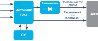
IGBT module control
IGBT modules are controlled by drivers. Microcircuits generate control pulses, ensure switching of keys in the required frequency range, and coordinate the operation of semiconductor devices with the control unit.
When choosing drivers for modules, manufacturers recommend following the following recommendations:
The voltage of the “collector-emitter” circuit to reduce dynamic losses and ensure stable operation of the transistor when the key is unlocked should be +15±10% V, when locked -7...-15 V. The maximum value is no more than ±20 V.
Intelligent Power Modules (IPM) based on the SLLIMM IGBT family from ST
The SLLIMM family of smart power modules are designed to meet the requirements of a wide range of end applications in the power range from 300 W to 2.0 kW, such as:
- Washing machines
- Dishwashers
- Refrigerators
- Air conditioner compressor drivers
- Sewing machines
- Pumps
- Power tools
- Low power industrial controls
IGBT-based Intelligent Power Modules (IPMs) expand ST's product range for power applications. These are solutions with superior thermal performance that simplify development by combining application-specific IGBTs and diodes, patented control functions, intelligent protection and many additional features.
IPM modules allow direct connection to microcontrollers, converting microcontroller output signals into high-power, high-voltage signals in the form necessary for controlling electric motors. A single module can replace more than 30 discrete components, significantly increasing reliability and reducing product size and cost. Figure 3 shows the benefits of replacing discrete components with an intelligent module.
Rice. 3. Benefits of replacing discrete components with an intelligent module
Each intelligent module includes the following units and components:
- Three-phase IGBT bridge inverter including:
- Six IGBTs with low loss and short circuit protection circuits,
- Six freewheeling diodes with low voltage drop and smooth recovery;
- Smart shutdown function
- Comparator for protection against current exceeding the maximum permissible value during a short circuit,
- Operational amplifier to increase the sensitivity of the current sensor,
- Three integrated clamping diodes,
- Mutual shutdown function
- Blocking in case of overvoltage;
ST's IPM modules use DBC (direct-bond copper) housings and vacuum welding processes, which guarantee better heat dissipation and lower electrical resistance, allowing for higher power densities and increased system reliability.
Powerful modules
Power transistors are manufactured not only as individual semiconductors, but also as assembled, ready-to-use modules. Such devices are part of powerful frequency converters for controlling electric motors. In each specific case, the diagram and principle of operation of the module will vary depending on its type and purpose. Most often, such devices use a bridge made of two power transistors.
Stable IGBT operation is ensured at a frequency of 150 kilohertz. As the operating frequency increases, losses may increase, which negatively affects the stability of electrical appliances. Power transistors exhibit all their advantages and capabilities when used with a voltage of more than 400 Volts. Therefore, such semiconductors are most often used in industrial equipment and high-voltage electrical appliances.
Krasnikov Nikolay
Source
Key Features and Benefits of IPM
Peculiarities
- 600V three-phase IGBT bridge inverter including switch control IC and freewheeling diodes
- IGBT short circuit protection
- Fully insulated housing made using DBC technology with increased heat dissipation
- Smart shutdown function
- Comparator for protection against current exceeding the maximum permissible value during a short circuit
- Operational amplifier to increase the sensitivity of the current sensor
- Built-in limiting diodes
- Small form factor
Advantages
- Convenient microcontroller control
- High efficiency and reliability
- Very low thermal resistance Rth
- Reduced number of components
- Optimized PCB topology
- Reduced PCB size (compact design)
- Low failure rate
- Ease of implementation of the field-driven control (FOC) algorithm without the use of additional sensors
Table 4 presents the main characteristics of ST's IPM.
Table 4. Main characteristics of ST intelligent power modules (IPMs)
| Peculiarities | Basic version | Full featured version | |||
| STGIPS10K60A | STGIPS14K60 | STGIPL14K60 | STGIPS20K60 | STGIPL20K60 | |
| Operating voltage, V | 600 | 600 | 600 | 600 | 600 |
| Operating current at TC=25 °C, A | 10 | 14 | 15 | 18 | 20 |
| RthJC max. For one IGBT, °C/W | 3,8 | 3 | 2,8 | 2,4 | 2,2 |
| Type of shell | SDIP-25L | SDIP-25L | SDIP-38L | SDIP-25L | SDIP-38L |
| Case size, mm (X, Y, Z) | 44,4×22,0×5,4 | 44,4×22,0×5,4 | 49,6×24,5×5,4 | 44,4×22,0×5,4 | 49,6×24,5×5,4 |
| DBC technology | Yes | Yes | Yes | Yes | Yes |
| NTC | Yes | Yes | Yes | Yes | Yes |
| Built-in limiting diodes | Yes | Yes | Yes | Yes | Yes |
| SD function | No | Yes | Yes | Yes | Yes |
| Comparator for short circuit protection | No | Yes (1 output) | Yes (3 pins) | Yes (1 output) | Yes (3 pins) |
| Smart shutdown function | No | Yes | Yes | Yes | Yes |
| Operational amplifier to increase the sensitivity of the current sensor | No | No | Yes | No | Yes |
| Mutual shutdown function | Yes | Yes | Yes | Yes | Yes |
| Overvoltage lockout | Yes | Yes | Yes | Yes | Yes |
| Open emitter configuration | Yes (3 pins) | Yes (3 pins) | Yes (3 pins) | Yes (3 pins) | Yes (3 pins) |
| Compatible with 3.3/5V logic input levels | Yes | Yes | Yes | Yes | Yes |
| Input signal for high-side IGBTs | High active level | High active level | High active level | High active level | High active level |
| Input signal for low-side IGBTs | High active level | Low active level | Low active level | Low active level | Low active level |
Selection of IGBT modules
Transistor modules are selected based on several main characteristics:
- Maximum collector current Ic. Manufacturers usually give 2 values. One at standard room temperature +25°C, the second at +80°C. The manuals show a graph of collector current versus temperature. You can use it to determine intermediate values.
- Collector-emitter voltage. The characteristic determines the class of the semiconductor element. When choosing, you must use the voltage class table of IGBT transistors for industrial networks.
- Operating maximum collector-emitter voltage. For stable operation of the module, peak values should not exceed 80% of the nominal value. Normal operating voltage should not exceed 60% of the rated voltage.
- Gate charge and saturation voltage. The characteristics are needed to calculate the driver and determine losses when the transistor is open.
To select IGBT semiconductor modules for converters, the following algorithm is recommended:
- Determination of the nominal and maximum DC link voltage.
- Selecting the module type by classification voltage.
| IGBT voltage classes for electrical networks | |||
| Mains voltage, V | 220 | 380 | 660 |
| IGBT voltage, V | 600 | 1200 | 1700 |
- Determination of the limiting current at the output of the converter.
- Selecting the maximum switching frequency for the output current limit.
- Select an IGBT module with a rated current not less than the limit value at the converter output.
- Calculation of static and dynamic losses in each module element at the maximum permissible IGBT temperature.
- Calculation of the maximum temperature of the radiator in the area where the module is installed.
- Calculation of total losses per module.
The temperature value is chosen with a reserve. If the calculated value of the permissible value is exceeded, it is necessary to select a module with a higher rated current. If there is a large margin, select an IGBT with a lower rated current and perform the calculations again.
Evaluation boards from ST
ST produces a range of IGBT-based evaluation boards and intelligent modules based on them. Table 5 shows the main distinguishing features of these boards.
Table 5. Evaluation boards based on IGBTs and modules from ST
| Name | Peculiarities | Appearance |
| STEVAL-IHM025V1 | 1 x IGBT SLLIMM STGIPL14K60 1 x Viper16 based converter 1 xIGBT STGP10NC60KD | |
| STEVAL-IHM027V1 | 1 x IGBT SLLIMM STGIPS10K60A 1 x Viper16 based converter 1 xIGBT STGP10NC60KD | |
| STEVAL-IHM028V1 | 1 x IGBT SLLIMM STGIPS20K60 1 x PWM SMPS VIPer26LD 1 x IGBT STGW35NB60SD | |
| STEVAL-IHM021V1 | 3 x L6390 smart PWM drivers 6 x STD5N52U power switching MOSFETs | |
| STEVAL-IHM023V1 | 3 intelligent L6390 PWM drivers 7 powerful switching IGBT STGP10NC60KD | |
| STEVAL-IHM024V1 | 3 intelligent L6390 PWM drivers 6 powerful switching IGBT STGDL35NC60DI |
The STEVAL-IHM028V1 universal evaluation board is designed based on ST's STGIPS20K60 three-phase bridge inverter intelligent module with 600V operating voltage and 20A operating current. The module has built-in comparators for hardware protection (such as overcurrent protection and overheating protection).
The STEVAL-IHM028V1 evaluation board has the following distinctive features:
- Complete solution for 2kW power inverter,
- Connection to a single-phase power network with a voltage of 90…285 V AC or to a DC source with a voltage of up to +400 V,
- Input voltage doubler for connection to low voltage AC power network,
- Input inrush current limiter with pass-through relay,
- Active braking device with overvoltage comparator;
- Current measurement with both three and one current sensor;
- Possibility of connecting Hall sensors or encoder,
- Tachometer input,
- Hardware protection against overheating and overcurrent,
- Active air cooling with automatic switching when temperature rises,
- Compact and safe design,
- A universal platform for subsequent experiments.
Scope of use
Today, IGBT transistors are used in networks with voltage ratings up to 6.5 kW, while ensuring safe and reliable operation of electrical equipment. It is possible to use an inverter, variable frequency drives, welding machines and pulse current regulators.
Heavy-duty IGBT varieties are used in powerful control drives for trolleybuses and electric locomotives. Their use makes it possible to increase efficiency, ensuring the smoothest possible operation of equipment, promptly controlling the output of electric motors to their full power. Power transistors are used in high voltage circuits. They are used in circuits for household air conditioners, dishwashers, power supplies in telecommunications equipment, and in automobile ignitions.
MOSFET transistors from ST
In addition to IGBTs, ST also produces MOSFET transistors, the parameters of the most outstanding of which are shown in Table 6.
Table 6. Super MOSFET transistors from ST
| Name | VDSS, V | RDS(on) (at VGS=10 V) max, Ohm | Drain current (Dc)(I_D) max, A | Power dissipation (PD) max, W | Switching charge (Qg) typical, nC | Peculiarities | Reverse recovery charge (Qrr) type (nC) | Reverse recovery time (trr) typ., nsec | Peak reverse current (IRRM) nom., A | Type of shell |
| STE70NM50 | 500 | 0,05 | 70 | 600 | 190 | – | – | 552 | 42 | ISOTOP |
| STW27NM60ND | 600 | 0,016 | 21 | 160 | 80 | Fast diode | – | – | – | TO-247 |
| STW62NM60N | 600 | 0,049 | 55 | 350 | 130 | – | – | – | – | TO-247 |
| STW77N65DM5 | 650 | 0,043 | 65 | 400 | 185 | Fast diode | – | – | – | TO-247 |
| STW77N65M5 | 650 | 0,038 | 69 | 400 | 185 | – | – | – | – | TO-247 |
| STY112N65M5* | 650 | 0,019 | 93 | 450 | 360 | – | – | – | – | Max247 |
| STY60NM50 | 500 | 0,05 | 60 | 560 | 190 | – | – | 552 | 42 | Max247 |
| STY80NM60N | 600 | 0,035 | 74 | 560 | 360 | – | – | – | – | Max247 |
| * Outstanding operating current with low on-resistance. |
High-voltage power MOSFET transistors also deserve special attention: n-channel with operating voltage up to +1500 V and p-channel with operating voltage up to -500 V. The main parameters of the transistors are presented in Table 7.
Table 7. High voltage MOSFET transistors from ST
| Name | VDSS, V | RDS (on) (at VGS=10V) max, Ohm | Drain current (Dc)(I_D) max, A | Power dissipation (PD) max, W | Gate switching charge (Qg) type, nC | Reverse recovery charge (Qrr) typ., nC | Reverse recovery time (trr) type, nsec | Maximum reverse current (IRRM) nom., A | Type of shell |
| n-channel with operating voltage +1500 V | |||||||||
| STFW3N150 | 1500 | 9 | 2.5 | 63 | 29,3 | – | – | – | TO-3PF |
| STFW4N150 | 1500 | 7 | 4 | 63 | 30 | – | – | – | TO-3PF |
| STP3N150 | 1500 | 12 | 2,5 | 140 | 18 | – | – | – | TO-220 |
| STP4N150 | 1500 | 7 | 3,1 | 160 | 35 | – | 510 | 12 | TO-220 |
| STW3N150 | 1500 | 9 | 2,5 | 140 | 29,3 | – | – | – | TO-247 |
| STW4N150 | 1500 | 7 | 4 | 160 | 30 | – | 510 | 12 | TO-247 |
| STW9N150 | 1500 | 2,5 | 8 | 320 | 89,3 | – | – | – | TO-247 |
| p-channel with operating voltage -500 V | |||||||||
| STD3PK50Z | 500 | 4 | -2,8 | 70 | 20 | – | – | – | DPAK |
Installation of IGBT modules
To effectively cool semiconductor modules, it is necessary to prepare the surface of the heatsink and ensure a tight fit of the device substrate to the cooler. The surface roughness should be no more than 10 microns, the deviation from parallelism should be less than 20 microns at a distance of up to 10 cm.
Before installation, you need to make sure that there are no solid particles on the surfaces, and also degrease the substrate and radiator with any solvent that is non-aggressive to the component materials.
To install the module, be sure to use thermal paste without solid inclusions. The characteristics of the material must be maintained at any operating temperature throughout its entire service life. The recommended temperature margin is 10%. Before applying the paste, the contact surfaces of the cooler and the substrate are degreased with a lint-free cloth soaked in a solvent. The thickness of the paste layer is adjusted with a special comb. When applying heat-conducting material, avoid getting it on the radiator and in the sockets for threaded connections.
Fastening of power models is carried out in the following order:
- The housing is secured with two diagonal bolts.
- A heat-conducting material is applied.
- Tighten the bolts diagonally (recommended torque 0.5 Nm ± 15%).
- Leave for half an hour to fill the voids with heat-conducting paste.
- Tighten the bolts with a force of 3-5 Nm.
For tightening, electronic tools with a low rotation speed and a force control function are used. You cannot use pneumatics; such a tool is not precise enough and can create excessive tightening force, which leads to stress on the device body and cracks in the semiconductor crystal.
During installation, it is prohibited to bend the power and control contacts, subject the device body to impacts, or apply excessive tightening forces.
Literature
1. ST. AN1491. IGBT BASICS. Link
2. ST. 600 V SiC diodes. Link
3. Link
4. Link
5. https://www.st.com/internet/analog/class/826.jsp
6. Link.
Obtaining technical information, ordering samples, delivery - e-mail
Where there are IGBT/MOSFET transistors, there are also gate drivers
In the line of analog and mixed integrated circuits produced by STMicroelectronics, MOSFET and IGBT transistor drivers occupy an important place. Early designs contain driver chips that control turning on or off a single MOSFET or IGBT transistor (category “Single” in STMicroelectronics terms, TD220, TD350 ). With a certain switching circuit, these drivers can control the load of both the upper and lower arms. We also note the TD310 chip - three independent single drivers in one package. This solution will be effective when controlling a three-phase load.
The most modern drivers are the L6384...L6388 and L639x series of high-voltage half-bridge drivers. These independent upper and lower side driver chips are controlled via the HIN and LIN inputs. Moreover, the high level of the logical signal turns on, respectively, the upper or lower arm of the driver. Some of these drivers use an additional SD input that disables both legs regardless of the state of the HIN and LIN inputs.
The STMicroelectronics L638xE Application Guide provides examples of a three-phase motor control circuit, a dimmable fluorescent lamp ballast circuit, DC/DC converters with various architectures, and a number of others. Also shown are diagrams of demonstration boards for all microcircuits of this family (including the topology of printed circuit boards).
L639x series drivers have additional functionality: operational amplifiers (in L6390 and L6392 ) are designed to measure the current flowing through the load. All microcircuits contain protection logic against the simultaneous opening of the upper and lower side transistors and, accordingly, the formation of a pause when the output state changes.
•••