Checking a bipolar transistor with a multimeter
The functionality of the bipolar transistor can be checked using a digital multimeter.
This device measures direct and alternating currents, as well as voltage and resistance. Before starting measurements, the device must be properly configured. This will allow you to more effectively solve the problem of how to test a bipolar transistor with a multimeter without desoldering. Modern multimeters can operate in a special measurement mode, which is why a diode icon is displayed on the body. When the question of how to check a bipolar transistor with a tester is decided, the device switches to the semiconductor testing mode, and one should be displayed on the display. The device terminals are connected in the same way as in resistance measurement mode. The black wire is connected to the COM port, and the red wire is connected to the output that measures resistance, voltage and frequency.
Older multimeters may not have a diode and transistor test feature. In such cases, all actions are carried out in the resistance measurement mode set to maximum. The multimeter battery must be charged before use. In addition, you need to check the serviceability of the probes. To do this, their tips are connected to each other. The squeak of the device and the zeros shown on the display indicate that the probes are working properly.
Checking a bipolar transistor with a multimeter is performed in the following order:
- First of all, you need to correctly connect the leads of the multimeter and the transistor. To do this, you need to determine exactly where the base, collector and emitter are located. To determine the base, a black probe is connected to the first electrode, which is presumably considered the base. Another red probe is alternately connected first to the second and then to the third electrode. The probes are swapped until the device detects a voltage drop. After this, the bipolar transistor is finally checked with a multimeter and the pairs are determined: “base-emitter” or “base-collector”. The emitter and collector electrodes are determined using a digital multimeter. In most cases, the voltage drop and resistance at the emitter junction are higher than at the collector junction.
- Definition of a base-collector pn junction: the red probe is connected to the base, and the black probe is connected to the collector. This connection operates in diode mode and allows current to flow in only one direction.
- Definition of a base-emitter pn junction: the red probe remains connected to the base, and the black probe must be connected to the emitter. Just as in the previous case, with this connection, current flows only when connected directly. This is confirmed by checking the NPN transistor with a multimeter
- Definition of an emitter-collector pn junction: if this junction is in good working order, the resistance in this section will tend to infinity. This is indicated by the unit shown on the display.
- The multimeter is connected to each pair of contacts in two directions. That is, transistors of the pnp type are checked by connecting them back to the probes. In this case, a black probe is connected to the base. After measurements, the results obtained are compared with each other.
- After checking the pnp transistor with a multimeter, the performance of the bipolar transistor is confirmed when, when measuring one polarity, the multimeter shows the final resistance, and when measuring the reverse polarity, one is obtained. This test does not require desoldering the part from the common board.
Many people are trying to solve the question of how to test a transistor without a multimeter using light bulbs and other devices. This is not recommended, since the element is highly likely to fail.
Why doesn't the transistor work?
The most likely reasons, according to experts, for the failure of the triode in the circuit are as follows:
- when one of the transitions disappears (breaks);
- transition breakdown;
- breakdown in one of the sections of the emitter or collector;
- loss of power by a semiconductor device during operation;
- visual damage to the transistor terminals.
Signs by which you can visually determine the breakdown of a triode in a circuit: darkening or change in the original color of the semiconductor device, a change in its “bulge” shape, the presence of a black spot.
How to test a transistorHow to test a transistor? (Or how to ring a transistor) Unfortunately, this question arises for everyone sooner or later. The transistor can be damaged by overheating during soldering or improper operation. If a fault is suspected, there are two easy ways to check the transistor.
The serviceability of any transistor, regardless of the type of device, can be checked using a simple multimeter. To do this, you must clearly know the type of element and determine the marking of its terminals.
Checking the transistor with a multimeter (tester) (transistor continuity) is carried out as follows. For a better understanding of the process, the figure shows a “diode analogue” of an NPN transistor. Those. The transistor seems to consist of two diodes. The tester is installed to test diodes and ring each pair of contacts in both directions. There are six options in total.
- Base–Emitter (BE): The connection must behave like a diode and conduct current in one direction only.
- Base to Collector (BC): The connection must behave like a diode and conduct current in one direction only.
- Emitter – Collector (EC): The connection must not conduct current in any direction.
When checking the PNP transistor, the “diode analogue” will look the same, but with inverted diodes. Accordingly, the direction of current flow will be reversed, but also only in one direction, and in the case of “Emitter – Collector” - in no direction.
Classification of transistors.
Scheme named after me, Siklai and Darlington.
To combine the above circuits into one, we will add some switching elements, a power supply, and for greater versatility, we will expand the range of emitter currents. The result is the following diagram of a device for testing transistors:
Click to enlarge
With the ratings indicated in the diagram, the calculated emitter current is provided already at +4V supply voltage, so this is truly a stable current generator. For the sake of experimentation, I connected transistors of the wrong structure a couple of times. Nothing burned! Although maybe it was worth asking more current? To be honest, few tests have been carried out on the endurance of this device, time will tell, but I like the beginning.
In principle, the device can be powered even from an unstabilized source, since current stabilization in the circuit is carried out over a very wide range of supply voltages. But! There are transistors (especially domestic ones) in which the base current transfer coefficient strongly depends on the collector-emitter voltage. To eliminate measurement errors due to an unstable network, the circuit provides a stabilized power supply. By the way, it is precisely because of such “curves” of transistors that measurements should be carried out at at least three different current values.
So, the circuit of the device for testing transistors turned out to be very simple, which allows you to easily assemble this device yourself, with your own hands. The device allows you to measure the base current transfer coefficient of low-power and high-power bipolar transistors “pnp” and “npn” structures by measuring the base current at a fixed emitter current.
For low-power bipolar transistors, the selected emitter current values are: 2mA, 5mA, 10mA. For high-power bipolar transistors, measurements are carried out at emitter currents: 50mA, 100mA, 500mA. No one forbids testing medium power transistors at currents of 10mA, 50mA, 100mA. In general, there are a lot of options. The values of the emitter currents can be changed at your discretion by recalculating the corresponding current-setting resistor using the formula:
R= Uо/Iе,
where Uo is the reference voltage of TL431 (2.5V), Ie is the required emitter current of the transistor under test.
ATTENTION: In nature there are TL431 microcircuits with a reference voltage of 1.2V (I don’t remember how the markings differ). In this case, the values of all current-setting resistors indicated in the diagram must be recalculated!
Checking digital transistors
A digital transistor is no different in appearance from a regular one, but the results of its “diagnosis” can confuse even an experienced technician. For many they were “incomprehensible” and remain so. In some articles you can find the statement - “testing digital transistors is difficult.
The best option is to replace it with a known-good transistor.” Undoubtedly, this is the most reliable method of verification. Let's try to figure out if this is really so. Let's figure out how to properly test a digital transistor and what conclusions to draw from the measurement results.
In the forward direction, the base-collector circuit of the transistor in question consists of a series-connected resistor R1 and the resistance of the base-collector junction itself. The junction resistance, since it is significantly less than the resistance of resistor R1, can be neglected.
This measurement will give a value approximately equal to the resistance value of resistor R1, which in our example is 10 kOhm. In the opposite direction, the junction remains closed and no current flows through this resistor. The avometer needle should show “infinity”.
The base-emitter circuit is a mixed connection of resistors R1, R2 and the resistance of the base-emitter junction itself (VD2 in Fig. 4 on the left). Resistor R2 is connected in parallel to this junction and practically does not change its resistance.
Therefore, in the forward direction, when the junction is open, the ampere-volt-ohmmeter will again show a resistance value approximately equal to the resistance value of the base resistor R1. When the polarity of the tester is changed, the base-emitter junction remains closed. Current flows through resistors R1 and R2 connected in series. In this case, the tester will show the sum of these resistances. In our example it will be approximately 32 kOhm.
As you can see, in the forward direction, a digital transistor is tested in the same way as a conventional bipolar transistor. The difference is that the arrow of the device shows the resistance value of the base resistor.
From the difference in the measured resistances in the forward and reverse directions, you can determine the resistance value of resistor R2.
Now let's look at testing the emitter-collector circuit. This circuit consists of two back-to-back diodes, and with any polarity of the tester, its arrow should show “infinity”. However, this statement is only true for a conventional silicon transistor.
In the case under consideration, due to the fact that the base-emitter junction (VD2) turns out to be shunted by resistor R2, it becomes possible to open the base-collector junction with the corresponding polarity of the measuring device. The transistor resistance measured in this case has some scatter, but for a preliminary assessment you can focus on a value that is approximately 10 times less than the resistance of resistor R1.
When changing the polarity of the tester, the resistance of the base-collector junction should be infinitely large. For a direct conduction transistor, the arrow will indicate “-” on the measuring device. As a measuring device, it is necessary to use pointer (analog) AVOmeters with a head deflection current of about 50 μA (20 kOhm/V).
Multifunction tester.
It should be noted that the above is somewhat idealized, and in practice, there may be situations that require logical interpretation of the measurement results. Especially in cases where the digital transistor turns out to be defective.
Checking the functionality of the field-effect transistor
This type of semiconductor elements is also called mosfet and mosfet components. Figure 4 shows the graphic designation of n- and p-channel field switches in circuit diagrams.
Figure 4. Field-effect transistors (N- and P-channel)
To test these devices, we connect the probes to the multimeter in the same way as when testing bipolar semiconductors, and set the test type to “continuity”. Next, we proceed according to the following algorithm (for an n-channel element):
- We touch the black wire to the “c” pin, and the red wire to the “i” pin. The resistance on the built-in diode will be displayed, remember the reading.
- Now you need to “open” the transition (this will only be possible partially), for this we connect the probe with the red wire to terminal “z”.
- We repeat the measurement carried out in step 1, the reading will change downwards, which indicates a partial “opening” of the field worker.
- Now you need to “close” the component, for this purpose we connect the negative probe (black wire) to the “z” leg.
- We repeat steps 1, the original value will be displayed, therefore, “closing” has occurred, which indicates the serviceability of the component.
To test p-channel elements, the sequence of actions remains the same, with the exception of the polarity of the probes, it must be reversed.
Note that insulated gate bipolar elements (IGBT) are tested in the same way as described above. Figure 5 shows the SC12850 component in this class.
Fig 5. IGBT transistor SC12850
For testing, it is necessary to perform the same steps as for a field-effect semiconductor element, taking into account that the drain and source of the latter will correspond to the collector and emitter.
In some cases, the potential on the multimeter probes may not be enough (for example, to “open” a powerful power transistor); in such a situation, additional power will be needed (12 volts will be enough). It must be connected through a resistance of 1500-2000 Ohms.
Checking thyristors on the multimeter connector for transistors
Many people are interested in whether it is possible to test a thyristor with a multimeter using the standard socket for testing transistors on the front panel, designated pnp/npn. The answer is yes. You just need to apply the correct voltage. The gain shown on the display will most likely be incorrect. Therefore, avoid being guided by numbers. Let's see how it's done. If the thyristor opens with a positive potential, it must be connected to pin B (base) of the npn half-socket. The anode is plugged into pin C (collector), the cathode is plugged into pin E (emitter). It is unlikely that it will be possible to test a powerful thyristor with a multimeter; for microelectronics, the technique will work.
Checking a MOSFET transistor with a digital multimeter
For example, let's take a field-effect transistor with an n-type channel IRF 640. You can see the graphic designation of such a transistor and its pinout in the following figure.
Before starting to test the transistor, short-circuit all its terminals to each other to remove any possible charge from the transistor.
Checking the built-in diode
First, you should prepare the multimeter and put it in diode testing mode. To do this, set the mode/limit switch to the position with the image of a diode.
In this mode, the multimeter, when connecting the diode in the forward direction (plus the device to the anode, minus the device to the cathode), shows the voltage drop across the pn junction of the diode. When the diode is turned on in the reverse direction, the multimeter shows “1”.
So, we connect the multimeter probes, as mentioned above, in the direct connection of the diode. Thus, we connect red noise (+) to the source, and black noise (-) to the drain.
The multimeter should show a voltage drop across the junction of the order of 0.5-0.7.
We change the polarity of connecting the built-in diode, and the multimeter, if the diode is working properly, will show “1”.
Checking the operation of the MOSFET transistor
The MOS transistor we are testing has an n-type channel, therefore, in order for the channel to become electrically conductive, it is necessary to apply a positive potential to the gate of the transistor relative to the source or drain. In this case, electrons from the substrate will move into the channel, and holes will be pushed out of the channel. As a result, the channel between the source and drain will become electrically conductive and current will flow through the transistor.
To open the transistor, the voltage on the multimeter probes in diode testing mode will be sufficient.
Therefore, we connect the black (negative) probe of the multimeter to the source (or drain), and touch the red one to the gate.
If the transistor is working properly, then the source-drain channel will become electrically conductive, that is, the transistor will open.
Now if you ring the source-drain channel, the multimeter will show some value of the voltage drop across the channel, due to the fact that current will flow through the transistor.
Thus, we place the black probe of the transistor on the source, and the red one on the drain, and the multimeter will show the voltage drop on the channel.
If you change the polarity of the probes, the multimeter readings will be approximately the same.
To close the transistor, it is enough to apply a negative potential to the gate relative to the source.
Therefore, we connect the positive (red) probe of the multimeter to the source, and touch the black probe to the gate.
In this case, the working transistor will close. And if you then ring the source-drain channel, the multimeter will only show the voltage drop across the built-in diode.
If the transistor is controlled by voltage from the multimeter (that is, it opens and closes), then we can conclude that the transistor is working.
Checking a MOSFET with a p-type channel is carried out in a similar way. With the exception that at all check points the polarity of connecting the probes is reversed.
I outlined in more detail and simply the entire method of testing a field-effect transistor in the following video tutorial:
Checking the varistor for serviceability with a multimeter and without a tester
Causes of malfunction
How to check a fuse with a multimeter
Varistors are installed parallel to the protected circuit, and a fuse is placed in series with it. This is necessary so that when the varistor burns out, if the overvoltage pulse is too strong, the fuse will burn out, and not the tracks of the printed circuit board.
The only reason for the failure of a varistor is a sudden and strong voltage surge in the network. If the energy of this jump is greater than the varistor can dissipate, it will fail. The maximum energy dissipation depends on the dimensions of the component. They differ in diameter and thickness, that is, the larger they are, the more energy the varistor can dissipate.
Voltage surges can occur during accidents on power lines, during a thunderstorm, or when switching powerful devices, especially inductive loads.
Verification methods
Any repair of electronics and electrical equipment begins with an external inspection, and then proceeds to measurements. This approach allows you to localize most faults. To find a varistor on the board, look at the figure below - this is what varistors look like. Sometimes they can be confused with capacitors, but can be distinguished by their markings.
If the element is burnt out and the markings cannot be read, look at this information on the device diagram. On the board and in the diagram it can be designated by the letters RU. The conventional graphic symbol looks like this.
There are three ways to test a varistor quickly and easily:
- Visual inspection.
- Call. This can be done with a multimeter or any other device that has a continuity test function.
- Resistance measurement. This can be done with a high-range ohmmeter, multimeter or megger.
A varistor fails when a large or prolonged current passes through it. Then the energy is dissipated in the form of heat, and if its amount is greater than that determined by the design, the element burns out. The housing of these components is made of a hard dielectric material, such as ceramic or epoxy coating. Therefore, when it fails, the integrity of the outer coating is most often damaged.
You can visually check the varistor for functionality - there should be no cracks on it, as in the photo:
The next method is to check the varistor with a tester in continuity mode. This cannot be done in the circuit, because the dialing can work through parallel-connected elements. Therefore, you need to unsolder at least one of its legs from the board.
Important: you should not check the elements for serviceability without desoldering them from the board - this may give false readings from the measuring instruments. Since in the normal state (without voltage applied to the terminals) the resistance of the varistor is high, it should not ring through
The test is performed in both directions, that is, by swapping the multimeter probes twice
Since in the normal state (without voltage applied to the terminals) the resistance of the varistor is high, it should not ring through. The test is performed in both directions, that is, by swapping the multimeter probes twice.
On most multimeters, the continuity mode is combined with the diode testing mode. It can be found by the diode icon on the mode selector scale. If there is a sound indication sign next to it, it probably also has a dial tone.
Another way to test a varistor for breakdown with a multimeter is to measure the resistance. You need to set the device to the maximum measurement limit, in most devices this is 2 MOhms (megaohms, designated as 2M or 2000K). The resistance must be equal to infinity. In practice, it can be lower, within 1-2 MOhm.
Interesting! The same can be done with a megaohmmeter, but not everyone has one. It is worth noting that the voltage at the megohmmeter terminals should not exceed the classification voltage of the component being tested.
This ends the available methods for checking a varistor. This time, the multimeter will help the radio amateur find the faulty element, as in a large number of other cases. Although in practice a multimeter is not always needed in this matter, because the matter rarely goes beyond a visual inspection. Replace the burnt element with a new one, designed for voltage and with a diameter no less than the burnt one, otherwise it will burn out even faster than the previous one.
Checking a Composite Transistor
Such a semiconductor element is also called a “Darlington transistor”; in fact, it is two elements assembled in one package. For example, Figure 6 shows a fragment of the specification for KT827A, which displays the equivalent circuit of its device.
Figure 6. Equivalent circuit of the KT827A transistor
It will not be possible to check such an element with a multimeter; you will need to make a simple probe, its diagram is shown in Figure 7.
Rice. 7. Circuit for testing a composite transistor
Designation:
- T is the element being tested, in our case KT827A.
- L – light bulb.
- R is a resistor, its value is calculated using the formula h21E*U/I, that is, we multiply the input voltage by the minimum gain value (for KT827A - 750), divide the resulting result by the load current. Let's say we use a light bulb from the side lights of a car with a power of 5 W, the load current will be 0.42 A (5/12). Therefore, we will need a 21 kOhm resistor (750 * 12 / 0.42).
Testing is carried out as follows:
- We connect the plus from the source to the base, as a result the light bulb should light up.
- We apply minus - the light goes out.
This result indicates the functionality of the radio component; other results will require replacement.
Checking a simple transistor circuit
Assemble a circuit with a transistor as shown in the figure. In this circuit, the transistor acts as a “key”. Such a circuit can be quickly assembled on a printed circuit board, for example. Pay attention to the 10Kohm resistor, which is included in the base of the transistor.
This is very important, otherwise the transistor will “burn out” during the test. If the transistor is working properly, then when you press the button the LED should light up and when released, it should go out. This circuit is for testing NPN transistors. If you need to check the PNP transistor, in this circuit you need to swap the LED contacts and connect the power supply the other way around.
Testing a transistor with a multimeter is simpler and more convenient. In addition, there are multimeters with a function for checking transistors. They show the base current, collector current and even the gain of the transistor.
Preparing tools
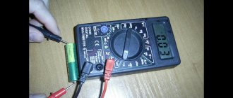
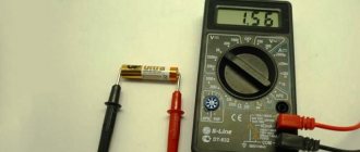
Every modern radio amateur has a universal tool called a digital multimeter. It allows you to measure direct and alternating currents and voltages, resistance of elements. It also allows you to check the functionality of circuit elements. Next to the switch for the “dialing” mode, as a rule, there is a diode and a speaker (see photo in Fig. 1).
Figure 1 – Multimeter front panel
Before checking the element, you need to make sure that the multimeter itself is working:
- The battery must be charged.
- When switching to semiconductor test mode, the display should show the number 1.
- The probes must be in good working order, since most devices are Chinese, and breaking the wire in them is a very common occurrence. You need to check them by leaning the tips of the probes against each other: in this case, zeros will appear on the display and a squeak will be heard - the device and probes are working.
- The probes are connected according to the color marking: the red probe goes into the red connector, the black probe goes into the black connector labeled COM.
If you do not know how to use this device, we recommend reading the detailed instructions for dummies on how to use a multimeter!
Multimeter design
A multimeter (tester) is a universal measuring device. It calculates current, voltage, resistance, and also determines the integrity of the wire. Multimeters are either analog or digital. The difference lies in the accuracy of the measurements and in the way you get the result: by reading by the movement of the hand according to the principle of a mechanical watch (analog), or by reading it on a screen (digital). Digital, for a number of reasons, is easier to use, and therefore is suitable for users with a minimum level of knowledge in radio electronics. Regardless of the type of tester, testing a transistor with a multimeter is a simple process.
Before starting diagnostics of the transistor, special attention should be paid to the correct configuration of the tester. This will only take a couple of minutes, but will protect you from errors in the results. So, the multimeter is equipped with two probes. Black is negative, red is positive. Be sure to make sure that each of them is inserted into the correct socket, because depending on the model and type of tester, there may be a different number of them. We check transistors exclusively in this position: the black probe is in the socket marked with the English letters COM, the red probe is placed in the connectors marked with the letters of the Greek alphabet.
If your feet smell bad, remember where they come from.
After googling a little, I found a diagram of a device for testing transistors, which was replicated on a fairly decent number of sites. Simple, portable... but no one except the author himself praises it. This should have been confusing right away, but alas.
So, the original circuit (with slightly simplified indication and switching):
Click to enlarge
According to the author's idea, here the operational amplifier together with the transistor under test forms a source of stable current. The emitter current in this circuit is constant and is determined by the value of the emitter resistor. Knowing this current, all we have to do is measure the base current, and then by dividing one by the other, obtain the value h21e. (in the author’s version, the scale of the measuring head was immediately calibrated in h21e values).
Two bipolar transistors at the op-amp output serve to increase the load capacity of the microcircuit when measuring high currents. The diode bridge is included in order to eliminate the need to reconnect the ammeter when switching from “pnp” to “npn” transistors. To increase the accuracy of selecting complementary pairs of bipolar transistors, it is necessary to select zener diodes (setting the reference voltage) with the stabilization voltages as close as possible.
I was immediately confused by the “not entirely correct” switching on of the operational amplifier with a single-supply supply. But the breadboard will endure everything, so the circuit was assembled and tested.
Shortcomings immediately emerged. The current through the transistor was highly dependent on the supply voltage, which never resembles a stable current generator. What the author of the circuit managed to select, while powering the device from a battery, remains a big mystery. As the battery discharges, the “exemplary” current will flow away and quite noticeably. Then I had to tinker with the “amplifier” at the op-amp output, otherwise the circuit would work unstably when measuring transistors of different powers. It was necessary to select the value of the resistor, and then I switched to a more “classical” version of the amplifier. And the bipolar (correct) power supply of the op-amp solved the problem with the floating current.
As a result, the diagram took the form:
Click to enlarge
But here another drawback has emerged - if you confuse the conductivity of the bipolar transistor (turn on “pnp” on the device, and connect the “npn” transistor), and when selecting from a large number of transistors, you will definitely forget to switch the device sooner or later, then one will fail from the transistors of the “amplifier” and you will have to repair the device. And why do we need difficulties with bipolar power supply, opamp, amplifier, etc.?
Types, classification of transistors
We avoid exploring the wilds. Know a simple rule: in bipolar transistors, carriers of both signs participate in creating the output current, in field-effect transistors - one. Definition of smart guys. Now we work with our fingers:
Transistor device
- Field-effect transistors are the beginning. When the Beatles took the stage, semiconductors began to replace vacuum triodes. In short, a pnp transistor is two crystal layers rich in positive carriers (silicon, germanium, impurity conductivity). While teaching physics lessons, the teacher often talked about how V-valent arsenic doped the silicon lattice, forming a new material. Let us add that the positive p-regions are fenced off by a narrow negative one (n-negative). Like a lump in my throat. A narrow isthmus, called the base, refuses to allow electrons (in our case, more like holes) to flow in the desired direction. A small negative charge appears on the control electrode, the collector holes (the upper p-region on traditional electrical circuits) can no longer be contained, literally tearing towards the applied voltage. Since the base is thin, using the accumulated speed, the carriers fly over the isthmus and are carried further - reaching the emitter (lower p-region), here they are carried away by the potential difference created by the supply voltage. Typical school explanation. The relatively small voltage of the control electrode is able to regulate the speed of a strong flow of holes (positive carriers) entrained by the supply voltage field. This is what the technology is built on. Electrons move towards the holes; transistors are called bipolar.
- Field-effect transistors are equipped with a channel of any type of conductivity that separates the source and drain regions (see figure above). The control electrode is called a gate. Moreover, the main material of the substrate, the gate, is opposite to the channel, source and drain. Therefore, positive voltage (see figure) prohibits the flow of charges through the transistor. The plus will pull (to the p-region) available electrons. Field-effect transistors are used much more often in electronics. In the figure, the gate is electrically connected to the crystal, the structure is called a control pn junction. It happens that the region is isolated from the crystal by a dielectric, which is often an oxide. Pure MOSFET transistor, in Russian - MOS.
Transistor test circuit
Using a multimeter, bipolar transistors are checked in normal mode. If the tester supports such an option, often called hFE, a round connector is mounted on the front panel, divided by a vertical line into two parts, where 4 sockets are labeled as follows:
- B – base.
- C – collector.
- E – emitter.
There are two emitter sockets to take into account the layout of the housing pins. The base can be on the edge or in the middle. Made for convenience. It makes no difference which socket the emitter leg of the bipolar transistor is inserted into. A few words on how to use it.
Construction and details.
Due to the simplicity of the device, no printed circuit board was developed; all elements are soldered to the pins of switches and connectors. The entire structure can be assembled in a small case; everything will depend on the dimensions of the transformer and switches used.
When testing powerful bipolar transistors at high currents (100mA and 500mA), they must be mounted on a radiator! If a plate radiator is mounted on one of the walls of the device or the radiator itself is used as a wall of the device, this will make using the device more convenient. A radiator that is always with you! This will significantly speed up the process of testing powerful transistors in TO220, TO126, TOP3, TO247 and similar packages.
The power supply stabilizer chip also needs to be installed on a small radiator. Any diode bridge is suitable for a current of 1A and higher. As a transformer, you can use a suitable small-sized one, with a power of 10 W or more with a secondary winding voltage of 10-14 V.
Optional: the device for testing transistors has sockets for connecting a second multimeter (included in the DC voltage measurement mode to a limit of 2-3V). I spotted this idea on one of the forums. This allows you to measure Ube of the transistor (if necessary, calculate the slope). This function is very convenient when selecting bipolar transistors of the same structure for PARALLEL connection in one arm of the amplifier output stage. If at the same current the voltages Ueb differ by no more than 60 mV, then such transistors can be connected in parallel WITHOUT emitter current equalizing resistors. Now do you understand why Accuphase amplifiers, where up to 16 transistors are connected in parallel in each arm in the output stage, cost so much money?
List of elements used:
Resistors: R3 - 820 Ohm, 0.25 W, R4 - 1k2, 0.25 W, R5 - 510 Ohm, 0.25 W, R6 - 260 Ohm, 0.25 W R7 - 5.1 Ohm, 5 W (more is better), R8 - 26 Ohm, 1 W, R9 - 51 Ohm, 0.5 W, R10 - 1k8, 0.25 W.
Capacitors:
C1 - 100nF, 63V, C2 - 1000uF, 35V, C3 - 470uF, 25V
Switching:
S1 - switch type P2K or biscuit for three positions with two groups of contacts for switching, S2 - switch type P2K, toggle switch or biscuit with one group of contacts for switching, S3 - switch type P2K or biscuit for two positions with four groups of contacts for switching, S4 - momentary button, S5 - power switch
Active elements:
T3 - transistor type KT3102 or any low-power npn type with high gain, D3 - TL431, VR1 - integrated stabilizer 7812 (KR142EN8B), LED1 - green LED, BR1 - diode bridge for a current of 1A.
Miscellaneous:
Tr1 is a transformer with a power of 10W or more, with a secondary winding voltage of 10-14V, F1 is a 100mA...250mA fuse, terminals (suitable available) for connecting measuring instruments and the transistor under test.
Checking with a multimeter
Before you start checking the serviceability of a field-effect transistor with a multimeter, it is recommended to take certain safety measures in order to prevent the transistor from failing. Field-effect transistors are highly sensitive to static electricity, so grounding must be done before testing them. To remove accumulated static charges from yourself, you should use an antistatic grounding bracelet worn on your hand. If you do not have such a bracelet, you can simply touch the radiator or other grounded objects with your hand.
The storage of field-effect transistors, especially those with low power, must be carried out in compliance with certain rules. One of them is that the terminals of the transistors during this period are in a closed state with each other. The configuration of the bases, that is, the location of the pins in different models of transistors, may differ. However, their labeling remains unchanged, in accordance with generally accepted standards. In English, gate means Gate, drain means Drain, source means Source, and the corresponding letters G, D and S are used for marking. If there is no marking, you must use a special reference book or an official document from the manufacturer of electronic components.
The test can be performed using a dial ohmmeter, but it will be more convenient and effective to test with a digital multimeter configured to test pn junctions. The resulting resistance value displayed on the display, at the x100 limit, will numerically correspond to the voltage at the pn junction in millivolts. After preparation, you can proceed to the actual verification. First of all, you need to know that a working transistor has infinite resistance between all its terminals. The device should show such resistance regardless of the polarity of the probes, that is, the applied voltage.
Modern high-power field-effect transistors have a built-in diode located between the drain and source. As a result, when solving the problem of how to test a field-effect transistor with a multimeter, the drain-source channel behaves similarly to a conventional diode. Use a negative black probe to touch the substrate - drain D, and a positive red probe to touch the source terminal S. The multimeter will show the presence of a direct voltage drop across the internal diode of up to 500-800 millivolts. In reverse bias, when the transistor is turned off, the device will show an infinitely high resistance.
Next, the black probe remains in place, and the red probe touches the gate terminal G and returns to the source terminal S. In this case, the multimeter will show a value close to zero, regardless of the polarity of the applied voltage. The transistor will open as a result of touch. Some digital devices may not show a zero value, but 150-170 millivolts.
If after this, without releasing the red probe, touch the black probe to the gate terminal G, and then return it to the drain substrate terminal D, then in this case the transistor will close, and the multimeter will again display the voltage drop across the diode. Such readings are typical for most p-channel devices used in video cards and motherboards. Checking p-channel transistors is carried out in the same way, only by changing the polarity of the multimeter probes.
Field effect transistor operating principle
Field effect transistor - circuit
How to test a transistor with a multimeter
Field-effect and bipolar transistors
Current stabilizer on a field-effect transistor
Transistor operating principle
General verification algorithm
How to test a transistor with a multimeter? In general, the algorithm looks like this:
- connect the multimeter probes in the standard way - black to the COM port, red to the port next to which there are the letters Ω, V and, possibly others (depending on the model);
- set the device to the maximum resistance mode - as a rule, this is 2000 Ohms, or to the “continuity” mode;
- make sure that the battery is charged, the insulation of the probe wires is not damaged, and the multimeter is working properly. To do this, in the dialing mode, you need to connect the contacts of both probes to each other - the squeak of the multimeter and a unit on the screen, indicating a resistance that is higher than the measurement limit, will mean that the device is working correctly.
Further verification steps will depend on what type of element needs to be checked. Basically, semiconductor elements of two types are used in electronics - bipolar and field-field.
Check on board
To check the transistor with a multimeter without desoldering, you need a multimeter with a diode continuity function. We move the switch to this position, the connection of the probes is standard: black to the common link (COM or with a ground symbol), red to the middle (socket for measuring resistance, current, voltage).
How to check a transistor with a multimeter without desoldering
To understand the principle of testing, we need to remember the structure of bipolar transistors. As already mentioned, they come in two types: PNP and NPN. That is, these are three consecutive areas with two transitions, united by a common area - the base.
The structure of a bipolar transistor and how it can be represented in order to understand how we will test it
Conventionally, we can imagine this device as two diodes. In the case of the PNP type they are turned on towards each other, in the case of NPN they are in mirror image. This representation is in the picture in the right column and in no way reflects the structure of this semiconductor device, but explains what we should see when making a call.
Testing a PNP type bipolar transistor
So, let's start by checking the PNP type bipolar. This is what we should get:
- If you apply a plus (red probe) to the base and a minus (black probe) to the emitter or collector, there should be an infinitely large resistance. In this case, the diodes are closed (see the equivalent circuit).
- If we apply minus to the base (black probe), and plus to the emitter or collector (red probe), we see a current from 600 to 800 mV. In this case, it turns out that the transition is open.
- If we touch the emitter and collector with the probes, there are no readings; in both options the transitions are locked.
So, the PNP transistor will be open only when positive is applied to the emitter or collector. If there are any deviations during testing, the element is inoperable.
Testing the serviceability of the NPN transistor
As you can see, in an NPN device the situation will be different. In practice it is diametrically opposite:
- If you apply a plus (red probe) to the base, and a minus to the emitter or collector, the junction will be open, and readings will appear on the screen - from 600 to 800 mV.
- If you swap the probes: plus to the collector or emitter, minus to the base, the transitions are locked, there is no current.
- When touching the emitter and collector with the probes, there should still be no current.
Checking the functionality of a bipolar NPN transistor with a multimeter
As you can see, this device works in the opposite direction. In order to understand whether a transistor is working or not, you need to know its type. This is the only way we can check the transistor with a multimeter without desoldering it from the board.
And once again we draw your attention to the fact that pictures with diodes do not in any way reflect the design of this semiconductor device. They are needed only to understand what we should see when checking transitions
This makes it easier to remember and understand the readings on the multimeter screen.
How to identify base, collector and emitter
Sometimes there are situations when you don’t have a reference book at hand and you don’t have the ability to find the pinout on the Internet, and the inscription on the transistor body has become unreadable. Then, using circuits with diodes, you can experimentally find the base and determine the type of device.
The structure of a bipolar transistor and how it can be represented to understand how we will test it
By searching, we look for the position of the probes at which all three electrodes “ring”. The conclusion regarding which the readings appear on the other two will be the base. Therefore, plus or minus is applied to the base, we determine the type, PNP or NPN. If we apply a plus to the base, it is an NPN type, if a minus is applied, it is a PNP.
To determine where the emitter is and where the collector is, you need to compare the multimeter readings during measurement. There is always more current at the emitter. So we will find the base, emitter and collector empirically.
Device Features
According to their design features, all transistors are:
- Bipolar (BT);
- Field or unipolar (PT);
- Composite (CT).
Before you start checking the integrity of a part with a digital multimeter, it is important to understand what a BT is. This is a three-layer semiconductor
Roughly speaking, these are 2 diodes connected to each other. Depicting it this way, it will be easier to understand the scheme for checking it on the board itself without desoldering.
In terms of conductivity, bipolar semiconductors are of two types:
- npn;
- pnp;
They are also most easily represented as diodes, photographs of which are often posted to explain the importance of understanding the structure and how it works. The output current occurs with the participation of holes and electrons - two carriers of different polarities, allowing them to be controlled.
The contacts involved in a semiconductor are called:
- base;
- emitter;
- collector.
The middle layer is connected to the base. To the emitter and collector - the extreme ones. The direction of the current is marked with an arrow. It is located near the emitter.
In a DC, the electric field is directed perpendicular to the current current. Their contacts are called as follows:
- gate;
- drain;
- source.
Also in their design there is an additional (conductive layer) for the flow of electric current through it.
PTs come in various modifications. With “p” or “p” channels, horizontal and vertical arrangement, near-surface and volumetric configuration.
How to test a semiconductor bipolar transistor
Before you start testing, you need to determine exactly what type of transistor you are currently testing. In addition to bipolar transistors, there are a great many other types of transistors, which need to be tested in a completely different way. Within the framework of this article, testing of bipolar type transistors will be considered. A bipolar transistor can be represented as an arrangement of 2 diodes. These diodes are connected into a half-bridge using electrodes of the same name. At the output of the transistor there are 3 electrodes, conventionally designated as base, collector and emitter. Depending on the polarity of the diode connection, NPN and PNP bipolar transistors are distinguished. The base-emitter junction is a control junction, and the collector-emitter junction is a driven junction. The transistor is designed in such a way that a small current signal, which is supplied to the base-emitter junction, with the correct ratio of resistors in the circuit of the collector, base and emitter junction, causes a higher current signal at the collector-emitter junction.
About the transistor
Let's remember that regardless of whether we are testing a transistor with forward or reverse conduction, they have two pn junctions. Any of these transitions can be compared to a diode. Based on this, we can confidently say that a transistor is a pair of diodes connected in parallel, and the place where they are connected is the base.
Thus, it turns out that for one of the diodes the leads will represent the base and collector, and for the second diode the leads will represent the base and emitter, or vice versa. The table below shows the color and code markings of low-power mid-frequency and high-frequency transistors.
Labeling table for low-power mid-frequency and high-frequency transistors.
Based on what was written above, our task comes down to checking the drop voltage on a semiconductor device, or checking its resistance.
If the diodes are operational, then the element being tested is working. First, let’s consider a transistor with reverse conductivity, that is, having an NPN conductivity structure.
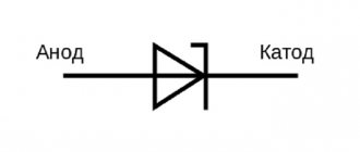
On electrical circuits of various devices, the structure of the transistor is determined using an arrow that indicates the emitter junction.
So if the arrow points to the base, then we are dealing with a forward conduction transistor having a pnp structure, and if on the contrary, then it is a reverse conduction transistor having an npn structure.
There are special probes for this, and even the multimeter itself has a socket for testing transistors, but, in my opinion, all of them are not entirely practical. To select a pair of transistors with the same gain (h21e), probes are a very necessary thing. And to determine serviceability, an ordinary cartoon will be enough.
To open a direct conduction transistor, you need to apply a negative voltage to the base. To do this, take a multimeter, turn it on, and then select the continuity measurement mode, usually indicated by a symbolic image of a diode. In this mode, the device displays the voltage drop in mV. Thanks to this, we can identify a silicon or germanium diode or transistor. If the voltage drop is in the range of 200-400 mV, then we have a germanium semiconductor, and if it is 500-700, a silicon one.
Modern multifunctional multimeter.
Checking the functionality of the transistor
We connect a positive probe (red) to the base of the field-effect transistor, connect another probe (black - minus) to the collector terminal and take a measurement. Then we connect the negative probe to the emitter terminal and measure. If the transistor junctions are not broken, then the voltage drop across the collector and emitter junction should be on the border from 200 to 700 mV.
To do this, we take and connect the black probe to the base, and connect the red one in turn to the emitter and collector, taking measurements.
Now let's make a reverse measurement of the collector and emitter junction.
During the measurement, the number “1” will be displayed on the device screen, which in turn means that in the measurement mode we have chosen, there is no voltage drop.
In the same way, you can check an element that is located on an electronic board from any device.
However, in many cases you can do without desoldering it from the board.
There are cases when soldered elements in a circuit are greatly influenced by low-resistance resistors.
But such schematic solutions are very rare. In such cases, when measuring the reverse collector and emitter junction, the values on the device will be low, and then you need to unsolder the element from the printed circuit board. The method for checking the functionality of an element with reverse conductivity (PNP junction) is exactly the same, only the negative probe of the measuring device is connected to the base of the element.
How to check a transistor without unsoldering it from the installation
You can check the transistor with a multimeter after checking the circuit to identify possible short-circuiting of the terminals of the element being tested with low-resistance resistors. If any are found, the part will have to be removed to check. If not, the check is performed using the methods described above, but the reliability of the testing will be low. Sometimes desoldering the base output is enough.
It is better to check field-effect transistors separately from the board. They are very sensitive to static electricity, so it is necessary to use an antistatic wrist strap.
Checking the built-in freewheeling diode
In almost any modern field-effect transistor, with the exception of special types, an internal “protection” diode is connected in parallel to the drain-source circuit. The presence of this diode inside the field device is due to the peculiarities of the technology for producing high-power transistors. Sometimes it interferes and is considered parasitic, but most field-effect transistors cannot do without it, as part of the integral structure of the electronic component.
Therefore, in a working field-effect transistor, this diode should also be working. In an n-channel field-effect transistor, this diode is connected with the cathode to the drain, and the anode to the source, and in a p-channel field-effect transistor, the anode is connected to the drain, and the cathode is connected to the source. Turn the multimeter into diode testing mode. If the field-effect transistor is n-channel, then attach the red probe of the multimeter to its source (source), and the black one to the drain (drain).
Transistors are one of the most widely used radioelements. Despite their reliability, they often fail due to irregularities in their operation. At the same time, searching for a faulty element due to the specific design of the field-effect transistor causes certain difficulties.
Typically the drain is in the middle and connected to the conductive substrate of the transistor, and the source is the right pin (check this in the datasheet). If the internal diode is working properly, the multimeter display will display a direct voltage drop across it - around 0.4-0.7 volts. If the position of the probes is now reversed, the device will show infinity. If everything is so, then the internal diode is working.
Measurement order.
Checking the drain-source circuit
The field effect transistor is controlled by the electric field of the gate. And if the gate-source capacitance is charged, then the conductivity in the drain-source direction will increase. So, if the transistor is n-channel, apply the black probe to the gate and the red one to the source, and after a second, reverse the orientation of the probes - red to the gate and black to the source. So we probably first discharged the shutter, and then charged it. The gate is usually on the left and the source is on the right.
Now move the red probe from the gate to the drain, and let the black probe remain at the source. If the transistor is working properly, then as soon as you move the red probe from the gate to the drain, the multimeter will show that there is a voltage drop at the drain - this means that the transistor has switched to a conducting state.
Now the red probe is on the source, and the black probe is on the gate (we discharge the gate with the opposite polarity), after which again the red probe is on the drain, and the black probe is on the source. The device should show infinity - the transistor has closed. For a p-channel field-effect transistor, the probes are simply swapped.
Checking the transistor without soldering.
If the device beeps
If at the drain-source testing stage the device beeps, this may be quite normal, because modern field-effect transistors have very low drain-source resistance when open. Alternatively, you can connect the gate to the source and in this position ring drain-source (for n-channel, red to drain, black to source), the device should show infinity.
The main thing is that there is no gate-source and drain-source ringing, especially at the moment when the gate is charged with the opposite polarity.
How to use a digital multimeter
In order to take measurements, the tester is connected with a set of wires to the element being measured. At one end of each wire there is a plug intended for installation in the meter socket, and at the other there is a contact probe. The procedure for measuring with an electronic multimeter can be generally represented as follows:
- Turn on the device by pressing the ON/OFF button.
- Insert the wire plugs into the corresponding sockets on the panel. COM - common socket for connecting a probe. V/Ω - positive socket for connecting a probe.
- Set the rotary switch to the diode continuity position “o)))”.
- Press the measuring probes to the terminals of the device.
- Take readings from the screen.
In addition to the continuity method, if the tester allows, you can measure the semiconductor element by setting the switch to the hFE position. In this case, wires and probes will not be needed. But this method is only suitable for bipolar devices.
Measuring the current gain of a bipolar transistor
If the tester has the ability to measure the current transfer coefficient, then you can check the operation of the transistor by installing the transistor leads into the corresponding sockets.
Current transfer coefficient is the ratio of the collector current to the base current.
The higher the gain, the more collector current can be controlled by the base current, all other things being equal.
The pinout (pin name) and other data can be taken from the data sheets (reference data) for the corresponding transistor. Data sheets can be found on the Internet through search engines.
The tester will show on the display the current transfer (gain) coefficient, which must be compared with the reference data.
The current transfer coefficient of low-power transistors can reach several hundred.
For powerful transistors it is significantly smaller - several units or tens.
However, there are powerful transistors with a transfer coefficient of several hundred or thousand. These are the so-called Darlington pairs.
A Darlington pair consists of two transistors. The output current of the first transistor is the input current for the second.
The overall current transfer coefficient is the product of the coefficients of the first and second transistors.
The Darlington pair is made in a common housing, but it can also be made from two separate transistors.
Basic parameters of the thyristor
To understand the principles of operation of this device and subsequent work with it, you need to know its main parameters, which include:
- The turn-on voltage is the minimum indicator of the anode voltage, upon reaching which the thyristor device will switch to operating mode.
- Forward voltage is an indicator that determines the voltage drop at the maximum value of the anode electric current.
- Reverse voltage is a measure of the maximum allowable voltage that can be applied to a device when it is in the closed state.
- The maximum permissible forward current, which refers to its maximum possible value during the time when the thyristor is in the open state.
- Reverse current, which occurs at maximum reverse voltage levels.
- Delay time before turning the device on or off.
- A value that determines the maximum electrical current to control the electrodes.
- The maximum possible power dissipation.
Safety precautions
For safety reasons, any testing and design with conventional and high-voltage diodes cannot be carried out in damp and damp rooms. In addition, it is impossible to make practically any switching measurements at the time of measurements and take measurements if the voltage and current values are greater than those indicated in the multimeter
Note! In order for the test to be easy, successful and not dangerous, according to the proven method of radio amateurs, it is necessary to use probes that have proper insulation
Safety precautions
In general, a transistor is a valve that reduces resistance and allows electric current to flow further along the circuit, moving from the collector device to the emitter. An element responsible for the operation of electrical appliances. It can be bipolar, isolated and field. You can check it with a multimeter without desoldering, as well as make repairs, following the instructions presented above.
Basic ways to check a transistor
The transistor is a very important element in most radio circuits. Those who decide to engage in radio modeling must first of all know how to test them and what devices to use.
A bipolar transistor has 2 PN junctions. The outputs from it are called emitter, collector and base. The emitter and collector are elements located at the edges, and the base is located between them, in the middle. If we consider the classical scheme of current movement, then it first enters the emitter and then accumulates in the collector. The base is necessary in order to regulate the current in the collector.