Soldering bga chips
How to solder boards? And how does BGA stand for? Bgacenter experts answer these two frequently asked questions during soldering courses. From English - ball grid arrey, that is, an array of balls that looks like a grid. Solder balls are applied to the microcircuit through a stencil, then a stream of hot air melts the solder itself and contacts of the correct shape are formed.
And the soldering process consists of a certain sequence of actions, following which we obtain a high-quality connection. But there are a large number of nuances for which people come to study. Starting with at what angle and at what distance from the board to hold the hair dryer nozzle, temperature conditions for dismantling and installing microcircuits, from which side to start the paddle. And during diagnostics, and there is an interlayer short circuit, nothing heats up. How to find the faulty element or circuit in this case? And many other subtleties that a current service center master can know. And the one who can confirm his level with completed repairs.
iPhone repair at Bgacenter
Dismantling of enclosures
Before you begin dismantling the old microcircuit, you should apply small marks along the edges of its body with some sharp object (a scalpel, for example). This procedure allows you to fix the location of the electronic component, which will greatly facilitate its subsequent installation.
To remove a faulty element, it is most convenient to use a thermal hair dryer, which can warm up all the legs at the same time (without the threat of damaging an already burnt chip).
In BGA dismantling mode, the heating temperature of the soldering zone should not exceed 320-350 degrees.
At the same time, the speed of the air stream is chosen to be minimal, which will prevent the melting of nearby contacts of small parts. While heating the legs, the hair dryer should be positioned strictly perpendicular to the treatment surface. In the case where there is no complete confidence in the malfunction of the part being removed, to maintain it in working condition, the jet flow should be directed not to the central zone, but to the periphery of the body part.
This precaution allows you to protect the chip crystal from overheating, to which memory chips of any computer equipment are especially sensitive.
After warming up for about a minute, you need to carefully pry the BGA chip by one of its edges with tweezers, and then slightly lift it above the circuit board. In this case, it is desirable to limit the applied force, clearly monitoring the moment of soldering of each of the contact pads.
Violation of this requirement can lead to damage to the landing spots of the microcircuit, which are part of the conductive tracks of the circuit board.
With a sudden, one-time force, a leg that is not completely sealed will certainly pull this pad along with it, and with it the entire track. As a result of such carelessness, the motherboard being restored can be permanently damaged.
Board and chip after desoldering
Soldering the chip
90% of the success of the repair depends on the correct dismantling of the microcircuits. It is at this stage that it is important not to tear off the nickels and not damage the microcircuit with high temperature. And they begin desoldering the chip by removing the compound.
Compound
Compound is a polymer resin, usually black or brown, used in the manufacture of telephone motherboards. Purpose of the compound:
- Additional fixation of radio components and bga chips on the board.
- Protection of non-insulated contacts from moisture.
- Increased board strength.
The most critical microcircuits, such as: CPU, BB_RF, EPROM, NAND Flash, Wi-Fi, are filled with compound at the factory after installation. And before dismantling, it is necessary to clear the perimeter of resin.
Removing the compound
Dismantling sequence
- Carefully inspect the board for previously performed repairs.
- Perform diagnostics and take the necessary measurements.
- Prepare the board for soldering, remove protective screens and stickers. Disconnect and remove the coaxial cable.
- Secure the motherboard in the appropriate holder.
- Remove the compound around the chip being removed. The temperature on the hairdryer is 210 – 240 degrees Celsius.
- Install heat sinks. The installation location of the heat sinks depends on the location of the soldered chip.
- Use a hairdryer to warm up the board for a few seconds. Thus, we increase the temperature of the board so that the flux spreads evenly.
- Apply FluxPlus, or any other no-clean flux, to the surface of the chip.
- Direct a stream of hot air onto the element to be soldered. Temperature during dismantling is 340 degrees Celsius. How can you tell when the solder has melted and it’s time to remove the chip from the board? There are several ways to do this: Track time using a stopwatch.
- Count down the seconds to yourself.
- “Push” with a probe or tweezers the microcircuit itself or the nearby harness (capacitors, resistors or coils). As soon as the chip being soldered begins to move, by a fraction of a millimeter, it is time to place the spatula under or use tweezers.
- Use a special spatula to remove any remaining compound;
How to perform bridge soldering, reballing or replacing a BGA chip
Step 1 - Laptop Diagnostics
By analyzing the reported malfunctions and the circumstances of their occurrence, which were indicated by the user at the time of the service request, the elements or components that can cause such symptoms are identified. When suspicion falls on the CPU or RAM, replacing these elements to check their serviceability is usually not a problem. However, when the BGA chip fails, such replacement is not possible.
Diagnosis of a damaged BGA can be done in three ways:
- Warming up a BGA chip with hot air
The BGA chip is heated by hot air at a certain temperature. A strictly defined temperature is used to prevent damage to the motherboard PCB. This procedure causes the microspheres under the core to expand and the functionality of the chip is temporarily restored.
I would like to emphasize that this method is used only to confirm your diagnosis and cannot be considered as a full repair of BGA chips. After cooling, the system malfunction usually returns. But sometimes it can be days or weeks later, so it is very important to have confidence in the service you are going to get your laptop repaired from.
Very often there are situations when unscrupulous service centers simply warm up the video chip, and the customer is told that they have completely soldered the chip. At the same time, they give a guarantee of no more than a month, and if the malfunction recurs, then they simply do another warm-up. And if warming up does not produce results (a fairly common situation), they say that you need to replace the laptop motherboard with a new one, since repairing the old one is not possible.
My workshop has all the necessary equipment for resoldering video chips, and I give a guarantee of 6 months.
- Diagnostics using X-ray control.
The motherboard is removed from the laptop and inserted into the X-ray machine. During diagnostics, the correct connection of each ball in the system is checked.
- Based on experience
Having worked in the laptop repair industry for many years, and handling a large number of repair orders, I am able to notice so-called “waves” of failure of the same BGA system in different brands and models of laptops. The service life or failure rates of the same model of BGA system are similar in all laptops where they are installed.
If I make a large number of replacements for a specific north bridge model in various laptop models, then I already know for the future that even in a seemingly working laptop, the bridge may soon fail.
Step 2 - Removing the BGA
When it is already known which BGA system is damaged, I proceed to dismantling the BGA chip from the board. In this case, the motherboard is installed in an infrared soldering station and a suitable thermal profile is selected using the software. To monitor the thermal profile, one or more thermocouples are installed. This process is fully automated.
Step 3 - Clearing Solder and Flux
At the next stage, a thorough cleaning of old solder and flux residues from the motherboard and the chip itself is carried out.
Step 4 — Preparing the New BGA Chip
If a chip is reballed, a stencil is attached to it and filled with balls. The video chip with the stencil is heated at the soldering station until the balls melt. If the video chip is replaced (the most recommended, but also costly repair method), then usually the balls are already knurled there.
Step 5 - BGA installation, soldering the chip to the motherboard
An infrared soldering station is also used for BGA installation. The appropriate solder profile for the new layout is selected, the new chip is positioned relative to the motherboard, and the chip is soldered. The BGA installation process is performed automatically.
Step 6 - Proper Cooling and De-Fluxing
After the system is installed, the motherboard must lose heat under appropriate conditions, otherwise the stresses caused by rapid heat loss may cause cracking and loss of connection paths on the circuit board. The gradual cooling process also occurs automatically at the soldering station.
When the correct cooling process is complete, the station beeps. All traces of flux in the immediate vicinity of the BGA are then removed. After proper component repair of the motherboard, there are no signs of interference.
Step 7 - Reassembling the Laptop After Repairing the Motherboard
After repairing the laptop motherboard, new thermal paste is applied to the chip. If necessary, the laptop's cooling fan is cleaned and lubricated to maximize cooling during operation.
Step 8 - Load testing and checking the laptop's functionality
Before a refurbished laptop is released into the hands of the owner, a total of 52 quality control tests are performed on it, which should detect possible repair errors or additional performance problems.
Soldering bga chips
The general principle of soldering is as follows: thanks to the surface tension created when the solder melts, the microcircuit is fixed relative to the contact pad on the system board. Soldering temperature for bga chips on iPhone boards is 320 – 350 degrees Celsius.
Preparing the chip:
- Use a special knife to clean the compound.
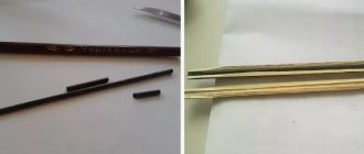
- Use a 1 or 2 mm copper braid (depending on the geometric dimensions of the chip) to remove any remaining solder.
- Restore the ball leads. There are two ways to form pins: BGA paste is applied through a stencil to the surface of the microcircuit (priority method) Used in most cases.
- Manually, with BGA balls. This option is suitable for chips with a small number of pins, up to 50. Although a few years ago, when the quality of stencils left much to be desired), modems on the iPhone 5S were rolled manually. That is, each ball was installed separately using a probe or tweezers. And this is 383 contacts, as calculated by ZXW. If, when distributing balls on a chip glued to a stencil, the balls are not fixed in the holes of the stencil; this means that not enough flux has been applied to the microcircuit.
SamsPcbGuide, part 11: Technologies - BGA-type cases, plastic and space
In the discussions for the previous article, proton17 wrote that ordinary BGAs do not fly into space, giving references to CCGA-type cases as an example of reliability. I decided to look into this issue and found a lot of interesting information (largely thanks to this ↓ person).
Despite their advantages (maximum number of pins in relation to dimensions at a given pitch, low lead inductance, self-alignment during soldering), BGA-type packages have a serious drawback for reliable applications - the impossibility of reliable visual control of the quality of solder connections.
The issue of the applicability of BGA components in reliable applications is not new; back in 1995, JPL conducted research into their reliability under various conditions. The results of the work were consistently presented in numerous publications by the real guru of this topic, R. Jafarian [1-5]. First, ceramic and “conventional” plastic housings were examined for surface flatness using laser scanning. The difference between the lowest and highest ball was chosen as a measure of flatness. The smaller this difference, the less likely there are defects during soldering. Ceramic packages had greater flatness, which also improved with fewer pins. This parameter is even more critical the higher the temperature of the solder used for soldering. The second stage is installation on printed circuit boards (FR-4 and polyimide) and thermal cycling. The electrical connections on the board and inside the test BGA package were organized in such a way as to form several groups of daisy chains. In each of these groups, the presence of connection failure was monitored by the criterion of exceeding a resistance of 1 kOhm for more than 1 μs. This criterion is defined in IPC-SM-785, however, it is not sufficient, since even a completely cracked connection may not go beyond the specified threshold due to contact pressure due to adjacent pins [4].
Due to the large difference in CTE between ceramic and FR-4/polyimide, CBGA packages failed earlier than plastic ones. Also, earlier failures showed plastic packages with a complete filling of the pin array, as opposed to packages with peripheral filling, since a local increase in the mismatch between the CTE of the package and the board occurs under the crystal, and it was there that the first failures in connections occurred.
Among the results, the influence of the glass transition temperature of the printed circuit board material on reliability for an extended temperature range is noted. FR-4 showed on average weaker results than polyamide. This result is confirmed in article [6]: the use of a printed circuit board FR-5 (with Tg ~ 170 oC and CTE ~ 13 ∙ 10−6 K−1) provides a fourfold increase in reliability compared to conventional FR-4 for a SON-type package .
It is worth noting that the CTE of a printed circuit board can differ even within the board and depends on its topology. Article [6] provides a wide range of values from 12 to 24 ∙ 10−6 K−1. There are also interesting data (Table 1) on the dependence of PBGA reliability on the diameter of the ball, contact pads (CP) on the board (NSMD type) and the base of the chip (SMD type). Their analysis reveals the following patterns:
- An increase in the diameter of the ball, all other things being equal, increased the number of thermal cycles withstood by ~20-30%.
- Increasing the diameter of the gearbox only on the side of the printed circuit board reduces reliability, since the height of the ball decreases. However, when the PBGA pad diameter is simultaneously increased, the reliability loss associated with the height reduction is compensated by the improvement in the communication area, and the overall effect becomes positive.
- Maximum reliability was obtained when the diameter of the CP on the board was slightly smaller than on the base of the microcircuit. The author refers to a similar result obtained in another work. Unfortunately, there are no comparative ones for the case with a large ball diameter.
Article [7] experimentally shows an increase in the number of thermal cycles withstanding with a decrease in the thickness of the ceramic base of the housing.
I was not able to familiarize myself with the previous article by one of the authors with a description of the process model, but the general considerations are as follows: the thinner the body, the less it resists tensile force, the less the load on the terminals. The rate of temperature change affects the primary location where defects occur in connections - at a fast rate (when local stresses arise), it is on the side of the case, at a slow rate (when the system has time to reach thermal equilibrium) - on the side of the printed circuit board. For the extended temperature range, the highest number of failures in ceramic CBGA packages was at the body (63Sn37Pb) and ball (90Pb10Sn) connection. So, the main obvious principles, experimentally confirmed back in 1995, for the reliability of BGA components are determined by thermal expansion and are as follows:
- The larger the case and the number of pins, the less reliability.
- The terminals furthest from the center are most vulnerable to destruction. For plastic BGA packages, in addition, the pins in the area where the crystal is located are vulnerable
- Ceramic cases on a printed circuit board made of textolite show low reliability. In addition, they do not align as well when soldering (as they have more mass) and are more sensitive to the quantity and quality of solder paste application, which complicates the process of reliable installation of components.
Lyrical digression. The use of printed circuit boards based on LTCC ceramics would eliminate the problem of CTE mismatch. Perhaps this is one of the directions for the development of electronic electronic equipment for space, which will lead to a reduction in the cost of such printed circuit boards.
Why use ceramic cases?
This issue was addressed by BarsMonster in one of the articles. The fact that in plastic jumpers are supported along the entire length by a compound, on the one hand, is logical, but on the other hand, the discrepancy between the CTE of the materials of the plastic case (compound, silicon, textolite, metal jumper) creates a large number of problems in an extended temperature range. Additional arguments for the use of ceramic cases are the CTE value close to silicon, high thermal conductivity, wide temperature range (which is also important for the assembly process), higher hydrophobicity, and an easier to master sealing process. On Spirit and Opportunity, it was ceramic cases that were used, but not the CBGA type, but the CCGA type (Fig. 1): in them, the balls were replaced with columns (sometimes reinforced with a copper spiral), which are capable of withstanding heavy loads (data is provided here that increasing the height by 2 times reduces mechanical stress and deformation by 30%). Despite the fact that these missions successfully completed and even exceeded their goals, it is worth noting that the high-performance processors in CCGA packages were located in a temperature-controlled unit. Articles [8, 9] present a comparison of CCGA and its corresponding PBGA under various conditions. For the CCGA-560, after 1075 thermal cycles of –50/75°C, the first contact failure occurred on the case side (an increased amount of solder paste was used for installation, which improved the reliability of the connection on the board side, see Fig. 2 and 3), while in PBGA-560 no failures were detected over 2000 cycles.
In order to reduce the load on the pins of BGA packages (including as a result of mechanical factors), several methods are used: corner-staking, compounding the space between the case and the board (underfill). However, the test results in [9] show that this technology not only does not eliminate the problem, but can, on the contrary, only worsen the resistance of the structure to the effects of temperature changes (Fig. 4).
The CCGA-717 housing with reinforced posts of smaller diameter was also tested [9]. Compared to CCGA-560 with non-reinforced leads, it showed greater resistance to thermal cycling: after 950 cycles of -55/100 oC there were no electrical failures, but defects on the leads had already begun to form (Fig. 5). The results of successful tests of CCGA-472 from the Aeroflex laboratory according to NASA standards are also publicly available.
Article [5] presents the results of a study of the influence of the final coating of a printed circuit board on the reliability of BGA components.
It was noted that for ENIG, unlike HASL and OSP, which exhibited ductile lead failure, some leads exhibited brittle lead failure. The IPC-9701A standard, which describes the methodology for testing the reliability of solder joints, prohibits the use of PCB coatings other than HASL, OSP and IAg, in order to avoid the influence of intermetallic compounds (also, by the way, the standard recommends the use of NSMD-type pads with mask indentation). As part of special studies [10, 11] on the problem of using ENIG as a finishing coating, it was not possible to detect any patterns and, thus, a decrease in the reliability of the connection is a difficult to predict event. Apparently for this reason, the standard does not recommend using such a finish. By the way, among others, ENEPIG coating was considered as an alternative coating, which showed good results ( in the original
- “performed very well and requires more testing”).
Table 2 summarizes the data from experiments to study the reliability of BGA-type components, the analysis of which indicates the presence of certain patterns (for example, reducing the thickness of the ceramic base significantly reduces the load on the terminals). These data can only act as a guideline for design, a reliability criterion - an experiment for a specific design and assembly technology. At the end of the article [9], valuable recommendations are given on the use of BGA components based on a summary of NASA experience from a person who has been dealing with the reliability of BGA components since 1995. Here are some points:
- Most PBGA packages provide sufficient reliability for missions with limited temperature variations (for example, controlled temperature within the module package). For long mission durations, packages with a large number of pins (more than 500) must be tested.
- Ceramic BGA packages with a small number of pins (less than 400) can meet reliability requirements for short-term missions with limited temperature variations, but for long-term missions must pass qualification testing even with reduced temperature differential requirements. For packages with a large number of pins (more than 500), testing is required in all cases.
- The use of underfill compound is not recommended for CCGA due to the high clearance between the package and the PCB. In the case of use, the CTE of the compound must be close to the CTE of the printed circuit board (load in the plane) and leads (load in the Z-axis direction), in addition, individual tests are required for each application.
- If it is necessary to increase resistance to mechanical stress, corner staking, edge bonding is more preferable for CCGA and CBGA packages compared to “underfill” technology. However, even here the reliability can be impaired by incorrectly selected materials.
There is other data: one of the JAXA presentations says that its use for CBGA packages increases the number of cycles before failure by an average of 1.7 times. Most often, “underfill” compounds are used in CSP-type packages, where the main task is to provide a transition between low CTE of silicon and CTE of a printed circuit board in dimensions as close as possible to the size of the crystal. For BGA components, as already mentioned, it is necessary to carry out tests in each specific case (without the possibility of transferring the results even if one of the parameters is changed, including technological ones) in accordance with the model of external influencing factors.
How many thermal cycles should the housing withstand? Of course, this depends on the model of influencing factors. With optimized assembly technology, many types of housings satisfy the generalized reliability criterion of no failures within 500 cycles of -60/125 °C (see Table 2). However, “not by thermal cycling alone,” the housing must not accumulate moisture, must provide low thermal resistance, must provide resistance to mechanical influences, etc. And according to the full list of criteria, ceramic cases have statistically higher reliability. Manufacturers of electronic components for space equipment, such as Aeroflex and MSK, produce their microcircuits in ceramic and metal-glass cases. Yes, for BGA-type execution, installation on textolite printed circuit boards creates problems due to non-compliance with the CTE, so it is necessary to invent ways to increase the reliability of connections - reducing the thickness of the base, using post leads, compounding, etc.
It is important to understand that the point is not in the packaging technology in general, but in whether a particular microcircuit meets the requirements of reliability and resistance to influencing factors. You can also use a commercial chip in a plastic case if it passes the full test cycle. At the same time, successful tests will not mean that the “same” microcircuit from a different manufacturer or even from a different batch will meet the reliability requirements. This is the difference between a reliable electronic component, which is included in the price - the manufacturer bears the costs of testing. The same 3D PLUS selects microcircuits in plastic for some of its microassemblies, but such products are already an order of magnitude more expensive. Another way is to perform testing and selection on the consumer side. This may be justified if the required functionality is not implemented in a reliable design, or if the external influence model and reliability requirements for the target mission are significantly lower than those typical on the market for reliable electronic components.
The request to reduce the mass of spacecraft (primarily the development of small-sized spacecraft) is pushing manufacturers to produce reliable electronic components in plastic cases; there are already solutions on the market (in addition, they are also advertised as low-cost ones). Perhaps in the near future, the amount of reliable, space-certified plastic will increase to meet the needs of low-Earth missions in low orbits, and ceramic cases will be transferred to LTCC printed circuit boards in order to roam deep space.
Literature
[1] Reza Ghaffarian, “BGAs for High Reliability Applications,” 1998. [2] Reza Ghaffarian, “Ball Grid Array Reliability Assessment for Aerospace Applications,” 1997 [3] Reza Ghaffarian, “Reliability and Failure Analyzes of Thermally Cycled Ball Grid Array Assemblies”, 1998 [4] Reza Ghaffarian, “Reliability of BGA Packages for Highly Reliable Applications and Chip Scale Package Board Level Reliability”, 1997 [5] Reza Ghaffarian, “Assembly Reliability Of BGAs And Effects Of Boards Finish”, 1998 [ 6] Jean-Paul Clech, “Solder Joint Reliability Of CSP Versus BGA Assemblies”, 2000 [7] Raj N.Master, Gregory B. Martin, etc. “Ceramic Ball Grid Array for AMD K6 Microprocessors Applications”, 1998 [8] Reza Ghaffarian, “Effect of Area Array Package Types on Assembly Reliability And Comments on IPC-9701A”, 2005 [9] Reza Ghaffarian, “CCGA packages for space applications ", 2006 [10] FDBruce Houghton. “ITRI Project on Electroless Nickel / Immersion Gold Joint Cracking”, 2000 [11] FDBruce Houghton. “Solving the ENIG Black Pad Problem: An ITRI Report on Round 2”, 1999
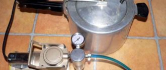
Bottom heating for bga soldering
To reduce the time the board is exposed to high temperatures, the boards are heated. We recommend the monoblock PCB heater STM 10-6. Stable maintenance of the set temperature over the entire area of the heating element contributes to uniform heating of the entire motherboard (depending on the heater model). And one more advantage over other thermal tables is a convenient universal fastening system.
Thermal table STM 10-6
Flux for BGA
| Interflux IF 8300-6 | Interflux IF 8300-4 |
One of the key factors for successful reballing is the correct flux. It is its properties that determine how the balls “stick” to the chip before heating, whether it will boil and foam during heating, and whether it will need to be washed off after mounting the chip on the board.
Therefore, BGA flux is the highest quality and most expensive type of flux. The use of other fluxes is extremely undesirable and can lead to negative results during restoration.
Flux for soldering bga
There are a huge number of flux manufacturers on the market. Bgacenter uses the widely used FluxPlus. You should pay attention to the date of manufacture and expiration date of the flux. Advantages of flux gel:
- without laundering (many masters recommend laundering anyway);
- convenient dispenser, hence high dosing accuracy during soldering work;
- does not emit unpleasant odors;
- ensures good spreading of solder over the base metal, thereby reducing the surface tension of the molten solder.
FluxPlus
Hot air soldering station
The purpose of the Quick 861DE ESD Lead station is soldering (disassembly and installation) of BGA microcircuits and SMD components. Advantages of this station:
- three memory modes CH1, CH2, CH3;
- high air-to-air performance, Quick 861DE is suitable for soldering circuit boards, phones and laptops;
- temperature stability.
What could be improved in the design of the station is temperature control not with buttons, but with rotary controls, as on the Quick 857D (W)+.
Quick 861DE ESD Lead
What are BGA chips
Depending on the purpose and device, microcircuits come in different sizes, which in turn affects the diameter and pitch of the balls.
For example, a bridge from a computer motherboard and a processor from a smartphone differ enormously (even less are the balls from the processor to the substrate).
Also, BGA chips are often coated with a compound for cooling, protection from moisture and mechanical stress, but this makes it much more difficult to replace such a chip.
Soldering iron
PS-900 METCAL – induction soldering system. A soldering iron power of 60 W is quite enough to work with multilayer boards of modern electronics. Phone repair engineers have 4 years of experience working with this particular soldering iron. What are the distinctive features of the PS-900:
- no need for calibration,
- large selection of tips,
- reliability of the station, the consumable material is the inductor. With daily intensive soldering, the inductor is replaced on average once every 10 months.
Soldering iron
What you need to organize soldering
The need for this procedure arises in cases where it is necessary to replace a burnt-out microcircuit, having previously unsoldered it from the seat.
Another option for the need for such operations is the independent production of printed circuit boards containing BGA type housings. To work using the BGA method, you will need the following tools and material:
- soldering station equipped with a hot air gun;
- easy-to-use tweezers;
- special solder paste and proprietary flux;
- stencil for applying solder paste, taking into account further positioning of the case;
- adhesive tape or braid to remove solder.
In some cases, a special suction can be used for these purposes to remove old solder.
For high-quality soldering of BGA packages, preliminary preparation of the footprint (also called the “working area”) is very important. Familiarity with the main technological features of this process will help you achieve the desired result.
Binocular microscope
For a novice phone repairman, the CM0745 microscope is a good option. Binocular microscope with a focal length of 145 mm (with a Barlow diverging lens installed). The purpose of the lens system is to increase the focal length while maintaining the working area.
Advantage of CM0745:
- Smooth increase is achieved using a ratchet.
- The lens system is made of glass, not plastic.
- Possibility to equip the microscope head with different tables and stands.
- Magnification up to 45X.
Microscope for soldering circuit boards
Solder quality
After completing the soldering work, you need to make sure that the bga soldering is done efficiently. Control is carried out in several ways:
- Visual.
- Measuring.
- Turning on the device.
- Connect to a laptop and check in 3uTools.
Read more about verification methods in the following material. For example, when diagnosing the iPad Air charging circuit by connecting the board to the LPS, with a working TRISTAR, the current consumption should be no more than 0.07 Amperes.
Cleaning and flux treatment
To follow the technology for soldering BGA packages at home, you need to familiarize yourself with the features of preparing the footprint for work. In this case, it should be assumed that even microscopic residues of removed solder should not remain in the soldering zone. To fulfill this requirement, it is most convenient to use a high-quality BGA flux made on the basis of alcohol and a small amount of rosin.
But first it is necessary to get rid of large particles of solder, which often remain in the mounting holes or between the contact pads (tracks). To do this, it is most convenient to use a copper screen braid, applied to the area to be cleaned and heated with a not very powerful soldering iron.
Application of alcohol rosin
For final cleaning of all extraneous “garbage,” liquid rosin diluted in alcohol is suitable, which is first applied to the soldering area and then heated with a regular soldering iron. Upon completion of assembling the remaining solder, the area for the microcircuit is thoroughly washed with the same alcohol or any natural solvent suitable for these purposes.
Board and microcircuit after washing