June 4, 2015
STMicroelectronicsarticleIGBT
STMicroelectronics produces several series of IGBT transistors and high-power fast-acting diodes that are ideal for creating welding machine inverters. State-of-the-art IGBTs of the V, H, HB, M series and W series diodes are characterized by low switching losses and low saturation voltage. These remarkable qualities were confirmed in practice when testing MMA inverters with a power of 4 and 6 kW.
The welding equipment market is a fast-growing power electronics industry. Today there are many types of welding machines:
- with various technologies - manual arc welding with a consumable electrode (manual metal arc, MMA), manual welding in a shielding gas environment (tungsten inert gas, TIG), semi-automatic welding in an environment of inert gases (MIG) or active gases (metal active gas, MAG);
- with various current sources - transformer, inverter;
- with direct current output (for example, for welding steel) or with alternating current (for example, for welding aluminum).
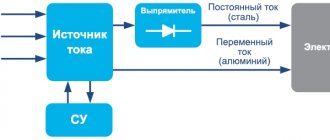
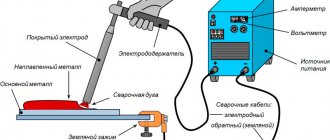
The most common type of welding technology is MMA. It is simple and is used in both professional and household devices. The structure of such a welding machine is quite simple and consists of a current source, an output rectifier (optional) and a control system (Figure 1).
Rice. 1. Simplified block diagram of the welding machine
The current source can be implemented on the basis of a powerful network transformer (transformer device), or on the basis of an inverter (inverter device). The main advantages of transformer devices are simplicity and maximum reliability, while the disadvantages are large dimensions, rough adjustment and poor welding quality. Inverter devices using modern semiconductor power switches do not have these disadvantages.
The main components of high-power inverters are IGBT transistors and high-speed diodes. The STMicroelectronics company produces power electronic components ideal for building welding machines [1]:
- V-series IGBTs with ultra-low turn-off energy, operating with voltages up to 600 V at frequencies up to 120 kHz;
- HB series IGBTs with low saturation voltage and low turn-off energy, operating with voltages up to 650 V at frequencies up to 50 kHz;
- H-Series IGBTs with low turn-off energy, operating with voltages up to 1200 V at frequencies up to 35 kHz;
- IGBT M series with low saturation voltage, operating with voltages up to 1200 V at frequencies up to 20 kHz;
- W series diodes with low forward voltage drop and minimal recovery time.
Requirements for IGBTs as part of welding inverters
The operating principle of an inverter welding machine is quite simple (Figure 2). The mains supply voltage is rectified and supplied to the inverter input. The inverter converts DC voltage into AC voltage, which is transmitted to the load through a high-frequency power transformer. The operation of the inverter is controlled by a control system (CS). By increasing and decreasing the duration of control pulses, you can change the power transmitted to the load. In addition to the main blocks, the circuit also contains auxiliary ones: a power factor corrector (PFC) and an output rectifier.
Rice. 2. Structure of inverter welding machine
The main block of an inverter welding machine is the inverter itself, which can be implemented using any of the known topologies. Among the most commonly used circuits are push-pull, bridge, half-bridge, half-bridge asymmetrical (oblique half-bridge).
Despite the variety of topologies, the requirements for IGBTs are approximately the same:
- High operating voltage. For a household network, the transistor voltage rating should be 600 V or higher.
- Large switching currents. Average values reach tens of amperes, peak values reach hundreds of amperes.
- High switching frequency. Increasing the frequency allows you to reduce the dimensions of the transformer and the inductance of the output filter.
- Low energy value for switching on (Eon) and switching off (Eoff) to minimize switching losses.
- Low value of saturation voltage Uke us. to minimize conducted losses.
- Resistant to harsh switching conditions. The inverter operates with an inductive load.
- Short circuit resistance. Critical for bridge and half bridge circuits.
To the above, it is worth adding that, firstly, when choosing transistors for an inverter, you should pay attention not only to the ratings of currents and voltages, but also to the parameters that determine power losses. Secondly, the requirements for low saturation voltage and high operating frequency are contradictory.
IGBTs manufactured by STMicroelectronics combine unique characteristics: they are capable of switching high power, are characterized by high performance, while maintaining a low value of Uke us. This became possible thanks to the use of the latest technologies.
Comparison of IGBT with MOSFET
The structures of both transistors are very similar to each other. Regarding current flow, an important difference is the addition of a P-type substrate layer under the N-type substrate layer in the IGBT module structure. In this additional layer, holes are introduced into the high-resistance N-type layer, creating an excess of carriers. This increase in conductivity in the N-layer helps reduce the overall on-state voltage in the IGBT module. Unfortunately, this also blocks the flow of electricity in the opposite direction. Therefore, a special diode is added to the circuit, which is located in parallel with the IGBT to conduct current in the opposite direction.
The MOSFET can switch at higher frequencies, however there are two limitations: the time it takes for the electrons to be transported in the drift region and the time it takes to charge/discharge the input gate and its capacitance. However, these transistors typically achieve higher switching frequencies than IGBT modules.
Power losses and features of IGBT production technology from ST
The main reason for inverter power limitation is IGBT overheating. It is a consequence of power loss dissipated in the form of heat.
As is known, the total power loss in an IGBT (Pd) consists of two components: conduction losses (Pcond, conducted losses) and switching losses (Pswitch) (Table 1).
Table 1. Power losses in IGBT
| Parameter | IGBT |
| Total losses | Pd = Pcond + Pswitch |
| Conducted losses | Pcond = Uke us (rms) × Ik × D, where D is the duty cycle |
| Switching losses | Pswitch = Eswitch × f, where f is the switching frequency, Eswitch = (Eon + Eoff) - the total switching losses (given in the IGBT parameters) |
| Maximum power limited by chip overheating | Pd = (Tj – Tc)/Rth-jc, where Tc is the case temperature, Tj is the crystal temperature, Rth-jc is the “chip-to-case” thermal resistance (given in the IGBT parameters) |
Conducted losses are determined by the value of the saturation voltage Uke us. For this reason, they try to reduce it as much as possible.
Switching losses combine the energy spent on switching on (Eon) and switching off (Eoff).
The turn-on energy of Eukl is largely determined by the built-in antiparallel diode. To optimize this parameter, you can use an external diode with better characteristics (shorter recovery time) or optimize the switching mode (switching at zero currents or voltages).
The turn-off energy Evykl is determined by the efficiency of minority carrier recombination in the IGBT structure. Delaying the recombination process leads to the appearance of a current tail (Figure 3), [2].
Rice. 3. Turn-off loss for planar IGBT
During the on state, current flows through the IGBT and an accumulation of minority carriers (holes from the p+ layer) occurs in its n- layer. After turning off the transistor, the number of these accumulated carriers decreases quite slowly, mainly due to ineffective recombination in the low-doped n- layer. As a result, a current “tail” is formed, leading to additional power losses.
One way to improve performance is to reduce the doping level of the p+ region. This leads to a decrease in the number of carriers, and hence to an accelerated recombination process. However, a decrease in the number of carriers will obviously lead to an increase in the saturation voltage.
Rice. 4. Development of IGBT technologies produced by STMicroelectronics
Thus, increasing performance while maintaining saturation voltage is possible only through qualitative improvements and the use of new technologies. For example, to speed up the recombination process, an n+ layer is created between the p+ and n- layers (Figure 4a). Performance increases, but remains quite low.
One of the revolutionary solutions that made it possible to qualitatively improve the characteristics of IGBTs was the use of TGFS (Trench Gate Field Stop) technology (Figure 4b). The essence of TGFS is to change the structure of the gate, which is performed in an isolated groove. The conductive channel becomes vertical, which reduces the effective thickness of the n- layer. This, on the one hand, leads to a decrease in the saturation voltage, and on the other, to a decrease in the number of accumulated carriers.
The most modern generation of IGBTs produced by STMicroelectronics V series includes all the best technological solutions [2]: TGFS, reducing the thickness of the original p-wafer, reducing the thickness of the diffuse and epitaxial layers, increasing the gate penetration depth (Figure 4c). This allows you to reduce the energy spent on shutdown while maintaining the saturation voltage value.
STMicroelectronics produces several series of IGBTs with different characteristics. A wide selection allows you to find the optimal transistors, taking into account the requirements for a specific welding machine and the topology used.
Specifics of using IGBT transistors in various applications
Requirements for power electronics devices are constantly increasing, providing for a decrease in the harmonic composition of currents and voltages and an increase in the efficiency of converter technology devices. One of the ways to satisfy these requirements is the correct choice of element base. This article uses Fairchild Semiconductor products to examine IGBT transistors for a variety of applications. The article is an abbreviated translation [1].
Introduction
IGBT transistors (hereinafter referred to as IGBTs) are in many ways similar to MOSFETs. For IGBTs the source material is P+, and for MOSFETs it is often N+. In MOSFETs, the n-type epitaxial layer is a region of high resistance. In IGBT, the n-type epitaxial layer is located on the P+ substrate, its conductivity is modulated and losses are lower. In Figure 1, these losses are reflected by the RDRIFT resistor. Typically, at high currents, the losses in a 600 V IGBT are lower than in a MOSFET with the same voltage.
| Rice. 1. IGBT circuit diagram |
IGBT, unlike MOSFET, is a bipolar transistor, therefore, recombination of minority carriers increases switching losses. Both types of transistors consist of many cells connected in parallel - Figure 1 shows the electrical circuit of an IGBT cell. The RSC resistance is extremely low, so the parasitic NPN transistor does not open even at very high currents. When the IGBT is fully open, the saturation voltage is determined from the relationships:
V CE(SAT) = VBE (PNP) + IMOSFET(RCH + RJFET + RDRIFT);
IMOSFET = IC/(hFE + 1).
The slope of the IGBT characteristic is much greater than that of the MOSFET, therefore the short circuit current (SC) is much greater, therefore, restrictive measures are necessary.
IGBT technologies The main two types of planar IGBTs are IGBTs with local breakdowns (punch-through, PT) and without local breakdowns (non-punch-through, NPT). The differences between them are illustrated in Figure 2. The PT structure has a thick P+ substrate and an N-buffer that controls injection into the N-region (the base of the pnp transistor). The switching time and VCE(SAT) value are determined by the degree of buffer doping and the lifetime of minority carriers - approximately 0.25 μs.
| a) b) Rice. 2. Structure of PT (a) and NPT (b) |
The NPT structure has a thick N-layer and no buffer. The switching time and VCE(SAT) value are determined by the injection of the P emitter, so the emitter is made very thin (less than 0.5 microns). The main differences between these structures are as follows. 1. Choice between VCE(SAT) and EOFF: in a PT structure it is usually possible to achieve a better compromise between these values due to a smaller N-layer thickness. 2. The temperature coefficient VCE(SAT) of an NPT structure is always positive, so it is convenient to connect such transistors in parallel. In an RT structure, the temperature coefficient can be either positive or negative, depending on what kind of impurity is used to reduce the lifetime of minority carriers. As a rule, fast transistors with a PT structure have a negative temperature coefficient, and slow ones have a positive one. 3. Temperature coefficient EOFF. For an NPT structure, EOFF increases slightly with increasing temperature, because The lifetime of minority carriers does not change. For transistors with a PT structure, EOFF increases significantly with increasing temperature - it doubles when the temperature rises from 25 to 150°C. Moreover, this effect is more clearly manifested in fast transistors. 4. TFALL. Transistors with an NPT structure have a fairly long decay time. On the contrary, for transistors with a PT structure this time is extremely short, therefore the EOFF value is also low, and, consequently, switching losses are low. 5. EON is practically independent of temperature for both structures. 6. Possibility of switching off during inductive load - Unclamped Inductive Switching (UIS). Transistors with an NPT structure are more stable in this regard because they have a wide N-layer. In this parameter they are close to MOSFETs. IGBTs with PT structure are less resistant to avalanche flashover unless they are specifically designed to improve UIS. As the dynamic characteristics of PT transistors improve, the UIS deteriorates. 7. Resistance to short-circuit currents - Short circuit withstand time (SCWT). This parameter determines the time during which the transistor must withstand the short-circuit current. And in this regard, transistors with an NPT structure have an advantage due to the wider N-layer, which increases the resistance of the transistor, thereby reducing the short-circuit current. Not long ago, Fairchild began producing new planar transistors with reduced crystal thickness - Field Stop IGBT, using a structure that is in many ways similar to SMPS IGBT. The UF/D series of planar transistors with reduced conduction losses and soft switching are designed for low switching frequency applications such as induction heating. SF series of new Field Stop IGBTs can replace SMPS IGBTs, it is suitable for high switching frequency applications such as power factor correctors, uninterruptible power supplies, etc. In solar inverters, efficiency is the most important indicator, and the SFD series is designed for them. Transistors of this series are superior to their closest analogs in both turn-off time and switching energy. Let's look at the requirements placed on transistors by various applications. For example, an electric drive is very demanding on power switches: – low voltage VCE(SAT) ; – soft switching on and off to reduce electromagnetic interference; – low slope of the characteristic to reduce short-circuit currents; – it is desirable to withstand a short-circuit current of more than 10 μs; – wide area of safe operation when switched off - Reverse Biased Safe-Operating-Area (RBSOA), exceeding 5-6 times the rated current value; – positive temperature coefficient VCE(SAT), which allows transistors to be connected in parallel; – VCE(SAT) parameters and turn-off losses should be optimized to increase the switching frequency; – turn-on losses must be reduced - it is necessary to simultaneously reduce the parameters Trr and Qrr - the time and charge of the reverse surge of the antiparallel diode of the transistor; – it is necessary to reduce the Miller effect: the ratio Qgd/Qgs should be minimal; – gate drive voltage VGE(th) should exceed 6 V to reduce the influence of noise; – dv/dt switching speed must be less than 7 kV/µs. Almost the same parameters should be for solar inverters and uninterruptible power supplies, but in these cases it is necessary to increase the switching speed. Sometimes a very low VCE(SAT) value is required at low switching frequencies. For these applications, Fairchild has developed a series of LSDs that sacrifice dynamic performance to reduce VCE(SAT). On the other hand, the same inverter topology may require transistors with improved dynamic parameters if, for example, fundamental frequency modulation is used. In this case, it is convenient to use Field Stop IGBT of the SFD series. 600-V IGBT series RUF/C3 have been developed for the electric drive. It will soon be replaced by the new RUF series of planar Field Stop IGBTs.
1200-V IGBT
Transistors at this voltage are used in many applications. In some of them, short-circuit currents do not occur; in others, on the contrary, this regime is often repeated. The market for uninterruptible power supplies for data centers and inverters for solar panels is currently actively growing. In both cases, the high efficiency of the converters is very important, because the cost of solar panels is quite high, and the volume of the data center market is very large and is estimated at $50 billion in the USA alone. Therefore, the low efficiency of inverters in this case means large losses and an increase in cost. IGBT transistors largely determine the efficiency of inverters and are an important component of these systems. The company's product line includes NPT IGBTs with reduced turn-off losses, specifically designed for these applications. Their use reduces the size of coolers, and, consequently, the size and cost of inverters. Table 1 shows the main parameters of Fairchild IGBTs manufactured using different technologies. For high-voltage DC/DC converters and DC/DC converters with FB-ZVS (zero voltage switching) topology, NPT2 planar technology is suitable - turn-off losses in this case are very small and are reduced by 40-60% compared to the previous generation; Conduction losses are also reduced.
Table 1. Comparison of IGBT technologies
| Technology | VCE(SAT), 25°С | VCE(SAT) 125°С | EOFF, µJ/A, ,25°С | EOFF, µJ/A, 125°С | Scwr,125°C | UIS, mJ, 25°С |
| NPT2 planar | 2,3 | 3,0 | 25 | 36 | >10 | >600 |
| NPT trench | 2,0 | 2,2 | 32 | 60 | <1 | >250 |
| Field stop trench | 1,7 | 2,0 | 81 | 130 | >10 | <5 |
NPT trench
These transistors are designed to reduce VCE(SAT) and turn-off losses, in addition, the current density is increased, hence the cost is reduced. In transistors made using this technology (see Fig. 3a), it was possible to achieve a compromise between the voltage VCE(SAT) and turn-off losses. And although this technology is quite outdated, due to its low cost it is still in demand.
| a) b) Rice. 3. Structure of trench (a) and Field Stop Trench (b) cells |
Field Stop Trench
Field Stop Trench is the latest technology (see Fig. 3b). Adding impurities to the Field Stop N-buffer allows you to significantly reduce the thickness of the base without changing the breakdown voltage. The thin base reduces conduction losses and also allows for a good compromise between turn-off losses and VCE(SAT) voltage. In terms of current density, this technology is comparable to trench-gate IGBT. Its main features are as follows: – the absence of an epitaxial layer reduces the cost of the transistor; – the manufacturing process is quite expensive, but by reducing the crystal size the cost can be reduced; – if necessary, you can add impurities that reduce the lifetime of minority carriers; – a good compromise between VCE(SAT) and SCWT; – excellent functional performance; – small value of VCE(SAT), the same as in transistors with a PT structure; – small value of UIS; – due to the high current density, in fewer cases it is necessary to resort to parallel connection of switches.
Conclusion
There is no ideal IGBT, all of whose parameters would be better than those of its analogues. In each transistor manufacturing technology, it is possible to achieve the optimal value of only some of the main parameters. The information provided in this article about the basic technologies allows you to select the appropriate transistor for various applications.
Literature
1. Sampat Shekhawat and Bob Brockway, The Application-Specific Power Semiconductors//Bodoґs Power Systems, October, 2008.
Review of IGBT series from ST
The IGBT line produced by STMicroelectronics contains four series, the representatives of which are most suitable for welding inverters. These are the V, HB, H, M series. All these transistors meet the above requirements and have excellent characteristics [1, 4]:
- high operating voltages – 600…1200 V;
- high switching currents – up to 80 A;
- record shutdown energy values – from 0.2 mJ;
- speed – up to 120 kHz;
- availability of versions with built-in high-speed antiparallel diode;
- availability of various housing versions (TO-247, D2PAK, TO-220 and others);
- resistance to short circuit impulses.
The M series is designed for switching voltages up to 1200 V and currents up to 40 A (Table 2). A distinctive feature of the series is its low saturation voltage (no more than 2.2 V) and low switching energy (from 1.2 mJ). This makes these transistors the optimal choice for inverters operating at frequencies up to 20 kHz.
Table 2. Characteristics of M-series IGBTs
| Name | Frame | Uke max., V | Ik max. at Tc = 100°C, A | Uke us. max., V | Eoff typ. at Tc = 125°C, mJ | Diode | Fmax, kHz | Pd max., W |
| STGW15M120DF3 | TO-247 | 1200 | 15 | 2,2 | 1,2 | There is | 20 | 283 |
| STGW25M120DF3 | TO-247 | 1200 | 25 | 2,2 | 2 | There is | 20 | 326 |
| STGW40M120DF3 | TO-247 | 1200 | 40 | 2,2 | 3 | There is | 20 | 468 |
| STGWA15M120DF3 | TO-247 LONG LEADS | 1200 | 15 | 2,2 | 1,2 | There is | 20 | 283 |
| STGWA25M120DF3 | TO-247 LONG LEADS | 1200 | 25 | 2,2 | 2 | There is | 20 | 326 |
| STGWA40M120DF3 | TO-247 LONG LEADS | 1200 | 40 | 2,2 | 3 | There is | 20 | 468 |
The H series is capable of switching voltages up to 1200 V and currents up to 40 A (Table 3). Compared to M-series transistors, H-series IGBTs have lower switching energy (from 0.85 mJ) and higher saturation voltage (up to 2.4 V). For this reason, they are suitable for higher frequency applications and are capable of operating at frequencies up to 100 kHz.
Table 3. H Series IGBT Specifications
| Name | Frame | Uke max., V | Ik max. at Tc = 100°C, A | Uke us. max., V | Eoff typ. at Tc = 125°C, mJ | Diode | Fmax, kHz | Pd max., W |
| STGW15H120DF2 | TO-247 | 1200 | 15 | 2,4 | 0,85 | There is | 50 | 260 |
| STGW15H120F2 | TO-247 | 1200 | 15 | 2,4 | 0,85 | No | 50 | 260 |
| STGWA15H120DF2 | TO-247 LONG LEADS | 1200 | 15 | 2,4 | 0,85 | There is | 50 | 260 |
| STGWA15H120F2 | TO-247 LONG LEADS | 1200 | 15 | 2,4 | 0,85 | No | 50 | 260 |
| STGW25H120DF2 | TO-247 | 1200 | 25 | 2,4 | 1,4 | There is | 50 | 375 |
| STGW25H120F2 | TO-247 | 1200 | 25 | 2,4 | 1,4 | No | 50 | 375 |
| STGW40H120DF2 | TO-247 | 1200 | 40 | 2,4 | 2,2 | There is | 100 | 468 |
| STGW40H120F2 | TO-247 | 1200 | 40 | 2,4 | 2,2 | No | 100 | 468 |
The HB series is not the main one for the construction of welding inverters, but its characteristics are also excellent (Table 4). The saturation voltage for these IGBTs is a record among all families and starts from 1.65 V. Switching energy, in many cases, does not exceed 0.6 mJ. The operating frequency for members of the family reaches 50 kHz.
Table 4. HB Series IGBT Specifications
| Name | Frame | Uke max., V | Ik max. at Tc = 100°C, A | Uke us max., V | Eoff typ. at Tc = 125°C, mJ | Diode | Fmax, kHz | Pd max., W |
| STGFW20H65FB | TO-3PF | 650 | 20 | 1,65 | 0,6 | No | 50 | 58 |
| STGFW30H65FB | TO-3PF | 650 | 30 | 1,65 | 0,6 | No | 50 | 58 |
| STGFW40H65FB | TO-3PF | 650 | 40 | 1,8 | 0,6 | No | 50 | 58 |
| STGW20H65FB | TO-247 | 650 | 20 | 1,65 | 0,6 | No | 50 | 260 |
| STGW30H65FB | TO-247 | 650 | 30 | 1,65 | 0,6 | No | 50 | 260 |
| STGW40H65DFB | TO-247 | 650 | 40 | 1,8 | 0,6 | There is | 50 | 283 |
| STGW40H65FB | TO-247 | 650 | 40 | 1,8 | 0,6 | No | 50 | 283 |
| STGW60H65DFB | TO-247 | 650 | 60 | 1,75 | 1 | There is | 50 | 375 |
| STGW60H65FB | TO-247 | 650 | 60 | 1,75 | 1 | No | 50 | 375 |
| STGW80H65DFB | TO-247 | 650 | 80 | 1,6 | 1,3 | There is | 50 | 469 |
| STGW80H65FB | TO-247 | 650 | 80 | 1,8 | 1,9 | No | 50 | 469 |
| STGWA80H65FB | TO-247 LONG LEADS | 650 | 80 | 1,8 | 1,9 | No | 50 | 469 |
| STGWT20H65FB | TO-3P | 650 | 20 | 1,65 | 0,6 | No | 50 | 260 |
| STGWT30H65FB | TO-3P | 650 | 30 | 1,65 | 0,6 | No | 50 | 260 |
| STGWT40H65DFB | TO-3P | 650 | 40 | 1,8 | 0,6 | There is | 50 | 283 |
| STGWT40H65FB | TO-3P | 650 | 40 | 1,8 | 0,6 | No | 50 | 283 |
| STGWT60H65DFB | TO-3P | 650 | 60 | 1,75 | 1 | There is | 50 | 375 |
| STGWT60H65FB | TO-3P | 650 | 60 | 1,75 | 1 | No | 50 | 375 |
| STGWT80H65DFB | TO-3P | 650 | 80 | 1,6 | 1,3 | There is | 50 | 469 |
| STGWT80H65FB | TO-3P | 650 | 80 | 1,8 | 1,9 | No | 50 | 469 |
Series V, as mentioned above, is the flagship in the STMicroelectronics range. Thanks to the latest technologies, these IGBTs have almost no current tail, and the turn-off energy is minimal - from 0.2 mJ (Table 5), while the saturation voltage does not exceed 2.15 V. All this allows the use of V series transistors in high-speed inverters with a maximum switching frequency of up to 120 kHz.
Table 5. V-Series IGBT Specifications
| Name | Frame | Uke max., V | Ik max. at Tc = 100°C, A | Uke us. max., V | Eoff typ. at Tc = 125°C, mJ | Diode | Fmax, kHz | Pd max., W |
| STGB20V60DF | D2PAK | 600 | 20 | 2,15 | 0,2 | There is | 120 | 167 |
| STGB20V60F | D2PAK | 600 | 20 | 2,15 | 0,2 | No | 120 | 167 |
| STGFW20V60DF | TO-3PF | 600 | 20 | 1,8 | 0,2 | There is | 120 | 52 |
| STGFW20V60F | TO-3PF | 600 | 20 | 2,15 | 0,2 | No | 120 | 167 |
| STGP20V60DF | TO-220AB | 600 | 20 | 2,15 | 0,2 | There is | 120 | 167 |
| STGP20V60F | TO-220AB | 600 | 20 | 2,15 | 0,2 | No | 120 | 167 |
| STGW20V60DF | TO-247 | 600 | 20 | 2,15 | 0,2 | There is | 120 | 167 |
| STGW20V60F | TO-247 | 600 | 20 | 2,15 | 0,2 | No | 120 | 167 |
| STGWT20V60DF | TO-3P | 600 | 20 | 2,15 | 0,2 | There is | 120 | 167 |
| STGWT20V60F | TO-3P | 600 | 20 | 2,15 | 0,2 | No | 120 | 167 |
| STGB30V60DF | D2PAK | 600 | 30 | 2,15 | 0,3 | There is | 120 | 260 |
| STGB30V60F | D2PAK | 600 | 30 | 2,15 | 0,3 | No | 120 | 260 |
| STGFW30V60DF | TO-3PF | 600 | 30 | 2,15 | 0,3 | There is | 120 | 58 |
| STGFW30V60F | TO-3PF | 600 | 30 | 2,15 | 0,3 | No | 120 | 58 |
| STGP30V60DF | TO-220AB | 600 | 30 | 2,15 | 0,3 | There is | 120 | 260 |
| STGP30V60F | TO-220AB | 600 | 30 | 2,15 | 0,3 | No | 120 | 260 |
| STGW30V60DF | TO-247 | 600 | 30 | 2,15 | 0,3 | There is | 120 | 260 |
| STGW30V60F | TO-247 | 600 | 30 | 2,15 | 0,3 | No | 120 | 260 |
| STGWT30V60DF | TO-3P | 600 | 30 | 2,15 | 0,3 | There is | 120 | 260 |
| STGWT30V60F | TO-3P | 600 | 30 | 2,15 | 0,3 | No | 120 | 260 |
| STGB40V60F | D2PAK | 600 | 40 | 2,15 | 0,5 | No | 120 | 283 |
| STGFW40V60DF | TO-3PF | 600 | 40 | 2,15 | 0,5 | There is | 120 | 62,5 |
| STGFW40V60F | TO-3PF | 600 | 40 | 2,15 | 0,45 | No | 120 | 60 |
| STGP40V60F | TO-220AB | 600 | 40 | 2,15 | 0,5 | No | 120 | 283 |
| STGW40V60DF | TO-247 | 600 | 40 | 2,15 | 0,5 | There is | 120 | 283 |
| STGW40V60F | TO-247 | 600 | 40 | 2,15 | 0,5 | No | 120 | 283 |
| STGWT40V60DF | TO-3P | 600 | 40 | 2,15 | 0,5 | There is | 120 | 283 |
| STGW60V60DF | TO-247 | 600 | 60 | 2,15 | 0,75 | There is | 120 | 375 |
| STGW60V60F | TO-247 | 600 | 60 | 2,15 | 0,75 | No | 120 | 375 |
| STGWT60V60DF | TO-3P | 600 | 60 | 2,15 | 0,75 | There is | 120 | 375 |
| STGFW80V60F | TO-3PF | 600 | 80 | 2,15 | 1,15 | No | 120 | 79 |
| STGW80V60DF | TO-247 | 600 | 80 | 2,15 | 1,15 | There is | 120 | 469 |
| STGW80V60F | TO-247 | 600 | 80 | 2,15 | 1,15 | No | 120 | 469 |
| STGWT80V60DF | TO-3P | 600 | 80 | 2,15 | 1,15 | There is | 120 | 469 |
| STGWT80V60F | TO-3P | 600 | 80 | 2,15 | 1,15 | No | 120 | 469 |
To name the IGBTs of the presented series, a code consisting of eight positions is used (Table 6). It contains the component type, package designation, family name, breakdown voltage, diode presence and its characteristics. It is worth noting that versions of transistors with a low voltage drop diode (DL index) are not suitable for use in welding inverters.
Table 6. Naming of IGBT manufactured by STMicroelectronics
| STG | W | 60 | V | 60 | D | F | 3 |
| Generation technology | |||||||
| Trench gate Field Stop technology | |||||||
Built-in diode:
| |||||||
Breakdown voltage code:
| |||||||
Series:
| |||||||
| Maximum current at 100°C | |||||||
| Frame: | |||||||
| F – TO-220FP | WA – TO-247 Long Led | ||||||
| FW –TO3FP | WT – TO-3P | ||||||
| P – TO-220 | Y – Max247 | ||||||
Most of the IGBT families presented are available in two versions: with a built-in high-speed diode and without it. The characteristics of these diodes are quite good. However, if necessary, it is necessary to use external diodes, for example, in an asymmetric bridge circuit. In this case, you should pay attention to the powerful high-speed diodes of the W series produced by STMicroelectronics.
Review of powerful W series diodes from ST
Powerful high-speed diodes of the W series are designed specifically for operation as part of high-power pulse converters with harsh switching conditions. For this purpose, their characteristics are optimized accordingly (Table 7):
- to reduce static power, the forward voltage drop is reduced (from 0.92 V);
- reverse voltage reaches 600 V;
- average current reaches 200 A;
- recovery time and reverse current are significantly reduced to reduce switching energy;
- Most diodes are available in dual versions.
Table 7. Powerful high-speed diodes produced by STMicroelectronics
| Name | Frame | Diodes in the housing | Urev max., V | Iav max., A | Udirect max. at current, V | trestore max., ns | Tcrystal max., °C |
| STTH20W02C | TO-247 | 2 | 200 | 10 | 1.05 (10 A) | 25 | 175 |
| STTH30W02C | TO-247 | 2 | 200 | 15 | 1.15 (15 A) | 27 | 175 |
| STTH60W02C | TO-247 | 2 | 200 | 60 | 0.92 (30 A) | 30 | 175 |
| STTH200W03TV1 | ISOTOP | 2 | 300 | 200 | 1.15 (100 A) | 50 | 150 |
| STTH60W03C | TO-247 | 2 | 300 | 30 | 1.15 (30 A) | 35 | 175 |
| STTH30W03C | TO-247 | 2 | 300 | 15 | 1.4 (15 A) | 25 | 175 |
| STTH200W04TV1 | ISOTOP | 2 | 400 | 200 | 1.55 (100 A) | 55 | 150 |
| STTH61W04S | TO-247 | 1 | 400 | 60 | 1.15 (30 A) | 55 | 175 |
| STTH100W04C | TO-247 | 2 | 400 | 100 | 1.2 (50 A) | 50 | 175 |
| STTH200W06TV1 | ISOTOP | 2 | 600 | 200 | 1.3 (100 A) | 75 | 150 |
| STTH100W06C | TO-247 | 2 | 600 | 100 | 1.15 (50 A) | 75 | 175 |
| STTH50W06S | TO-247 | 1 | 600 | 50 | 1.75 (50 A) | 45 | 175 |
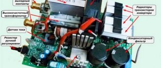
Results of practical application of IGBT from ST in MMA inverters
To confirm the advantages of IGBT transistors manufactured by STMicroelectronics, welding inverters were built and tested: MMA160 (input power 3.8 kW) and MMA200 (input power 6 kW) [3].
The test conditions were the same [3]:
- in both cases, an asymmetrical half-bridge inverter circuit with paired parallel IGBTs was used (Figures 5 and 6);
- mains voltage 220 V, 50 Hz was used as power supply;
- The ambient temperature was 25°C;
- Ceramic resistors with a total resistance of 145 mOhm with active cooling were used as a load;
- the maximum fill factor did not exceed 50% to ensure that there is no possibility of saturation of the output RF transformer core;
- protective shutdown was carried out when the transistors reached a temperature of 105°C.
The MMA160 inverter was built on the basis of STGW40V60DF transistors (Figure 5). The switching frequency was 63 kHz.
Rice. 5. MMA160 inverter circuit
During the tests, measurements were taken of input power, input current and transistor housing temperature. When the input power increased from 2 kW to a maximum power of 3.8 kW, the transistors warmed up and the turn-off energy increased (Table 8).
Table 8. Test results of the MMA 160 inverter
| Input power, kW | Input current, A | Power factor | Temperature, °C | Time | Switch-off energy, mJ |
| 2 | 15,4 | 0,58 | 62 | – | 311 |
| 3 | 22,2 | 0,61 | 83 | – | 466 |
| ~3.8 (max) | 26,3 | 0,66 | 105 | 10 min 17 sec | 550 |
The inverter showed stable operation over the entire power range. The shutdown at maximum power occurred only after 10 minutes 17 seconds, after the overheating protection (105°C) was activated. The maximum energy value for turning off the IGBT increased from 311 mJ to 550 mJ, which is a good result and corresponds to the value stated in the documentation (Table 5).
The MMA200 inverter was built using twin STGW60H65DFB IGBTs (Figure 6). The operating frequency was 63 kHz. For additional protection of transistors, snubber RC circuits were used.
Rice. 6. MMA200 inverter circuit
During testing, the MMA200's input power was increased from 2.6 kW to 5.8 kW. The inverter demonstrated stable operation in all modes and turned off after the temperature protection was activated 8 minutes 15 seconds after reaching a power of 5.8 kW. As the input currents increased, the transistor temperature increased and the turn-off energy increased (Table 9). The range of energy changes during shutdown was 586...947 mJ, which corresponds to the declared value.
Table 9. MMA200 inverter test results
| Input power, W | Output current, A | Output power, W | Temperature, °C | Time | Switch-off energy, mJ |
| ~2683 | 90 | ~2233 | 59 | – | 586 |
| ~3864 | 130 | ~3172 | 71 | – | 787 |
| ~4949 | 165 | ~3997 | 87 | – | 887 |
| ~5883 | 200 | ~4624 | 105 | 8 min 15 sec | 947 |
The tests carried out confirmed the excellent characteristics declared by the manufacturer. Thus, IGBTs manufactured by STMicroelectronics are ideal for building inverters for welding machines.
Evaluation boards from ST
ST produces a range of IGBT-based evaluation boards and intelligent modules based on them. Table 5 shows the main distinguishing features of these boards.
Table 5. Evaluation boards based on IGBTs and modules from ST
| Name | Peculiarities | Appearance |
| STEVAL-IHM025V1 | 1 x IGBT SLLIMM STGIPL14K60 1 x Viper16 based converter 1 xIGBT STGP10NC60KD | |
| STEVAL-IHM027V1 | 1 x IGBT SLLIMM STGIPS10K60A 1 x Viper16 based converter 1 xIGBT STGP10NC60KD | |
| STEVAL-IHM028V1 | 1 x IGBT SLLIMM STGIPS20K60 1 x PWM SMPS VIPer26LD 1 x IGBT STGW35NB60SD | |
| STEVAL-IHM021V1 | 3 x L6390 smart PWM drivers 6 x STD5N52U power switching MOSFETs | |
| STEVAL-IHM023V1 | 3 intelligent L6390 PWM drivers 7 powerful switching IGBT STGP10NC60KD | |
| STEVAL-IHM024V1 | 3 intelligent L6390 PWM drivers 6 powerful switching IGBT STGDL35NC60DI |
The STEVAL-IHM028V1 universal evaluation board is designed based on ST's STGIPS20K60 three-phase bridge inverter intelligent module with 600V operating voltage and 20A operating current. The module has built-in comparators for hardware protection (such as overcurrent protection and overheating protection).
The STEVAL-IHM028V1 evaluation board has the following distinctive features:
- Complete solution for 2kW power inverter,
- Connection to a single-phase power network with a voltage of 90...285 V AC or to a DC source with a voltage of up to 400 V,
- Input voltage doubler for connection to low voltage AC power network,
- Input inrush current limiter with pass-through relay,
- Active braking device with overvoltage comparator;
- Current measurement with both three and one current sensor;
- Possibility of connecting Hall sensors or encoder,
- Tachometer input,
- Hardware protection against overheating and overcurrent,
- Active air cooling with automatic switching when temperature rises,
- Compact and safe design,
- A universal platform for subsequent experiments.
Literature
- Products and solutions for Factory automation and control. STMicroelectronics, 2015;
- Giuseppe Introvaia. TA0350. Technical article. New trench gate field-stop V series: the real tail-less IGBT. Rev. 1. STMicroelectronics, 2013;
- Anselmo Liberti, Rosario Gulino. AN4638. Application note. Welding machines: V and HB series IGBTs on two-switch forward converters. Rev. 1. STMicroelectronics, 2015;
- https://www.st.com/.
Obtaining technical information, ordering samples, ordering and delivery.
•••