Alloys with bismuth
Solder made from tin, silver and small amounts of bismuth has the best solderability.
Sometimes germanium is added instead of bismuth. The lead-free alloy has a low melting point, which falls within the range of 200 to 210 ℃. The value may vary depending on the ratio of metals. Additives improve the wetting of parts with the melt and contribute to the formation of high-quality seams.
The melting point of a mixture of tin, zinc and bismuth is very close to that of lead solders. The advantage of a lead-free alloy is the absence of a toxic component.
However, zinc, as an active metal, causes many problems. Solder paste can be used quickly and changes during storage.
Soldering with such a lead-free product must be done using fluxes in an atmosphere of inert gases. Otherwise, there is a high probability of oxidation and excessive slagging of the seam.
Directions for use
The possibilities for soldering with lead-free solders are great. They include wave soldering or in special ovens.
You can use a regular soldering iron. The choice of technology is determined by the object, the operating conditions of the soldered product, and the specifics of production.
When working at defense enterprises, high-quality mixtures of tin, silver, and copper are recommended, to which antimony is added if necessary.
The presence of antimony worsens the environmental safety of the alloy. This is a very toxic element, mixtures with which are used only in cases of urgent need.
For working with professional equipment in industry and communication systems, solders made of tin, silver, copper or only tin-silver compositions of a eutectic nature are also suitable.
For office equipment, audio and video equipment, compositions based on tin, silver with or without the addition of copper or antimony are also recommended. Solders containing bismuth are used much less frequently for reasons of saving money.
General requirements
The number of metal compositions that do not include lead is constantly increasing. Thanks to many years of practical use, several basic compositions have become famous. Many of them are characterized by the eutectic phenomenon.
It lies in the fact that the melting point of an alloy with a carefully selected ratio of metal components is lower than that of any other mixture of selected metals. The eutectic qualities of lead-free solder make it possible to reduce the heating temperature of the working area and save the amount of electricity consumed.
There are general requirements for lead-free solders - the absence of unnecessary impurities. Foreign metals negatively affect the quality of the seam:
- if the alloys contain small amounts of nickel, the weld may have cavities;
- aluminum impurities will result in a dull and grainy compound;
- iron significantly increases the likelihood of scale formation;
- copper in excess tends to increase wettability;
- Antimony can cause the formation of a seam that is brittle at low temperatures.
It is important to use solders made by reputable manufacturers. At enterprises professionally involved in the production of lead-free solder alloys, much attention is paid to monitoring the cleanliness of all components
You can trust the quality of such products.
Menu
The symposium program was rich and extremely interesting. On the first day, presentations were made by experts from Sweden: Lars-Olaf Wallin, IPC representative in Europe, and Lars-Gunnar Klang, an independent expert in the field of soldering. On the second day - Werner Engelmaier, Chairman of the IPC Main Committee on Product Reliability, USA, and on the third, final day, reports were read by Russian specialists: Nikolai Ivanov, Deputy General Director for New Equipment and Technology of Avangard OJSC; Vladimir Ivin, head of the radio technology department of the same enterprise, and Stanislav Gaft, technical director of JSC OSTEK Enterprise.
Now let’s tell you more about each of the speakers and their speeches.
Lars-Olaf Wallin is a lecturer at the Royal Institute of Technology. Lars-Gunnar Klang is an independent soldering expert with 20 years of experience and a consultant on the transition to lead-free soldering technologies.
The reports by Lars-Olaf Wallin and Lars-Gunnar Klang dealt with the problems of lead-free and mixed installation technologies. The performances were divided into several parts.
At the beginning, issues related to the design stage of printed circuit boards (hereinafter PP) and printed circuit assemblies (hereinafter PU) were considered. Thus, issues of designing printed circuit boards from the point of view of their further assembly and testing were touched upon. Once again, the problems that arise when developers and designers want to place complex functionality in a small volume were pointed out, which necessitates the “dense” placement of components and multilayer PCB structures.
To resolve design issues - the dimensions of contact pads (hereinafter referred to as CP) of components and the gaps between them and the conductive pattern - it was recommended to be guided by IPC-7351A (Fig. 1).
Rice. 1.
Options for changing the gearbox in accordance with IPC-7351A, depending on the installation density for: a) chip components; b) components with gullwing terminals
Examples were given of defects that arise due to incorrect design and in the case when the capabilities of the PCB manufacturer are not taken into account (Fig. 2).
Rice. 2.
Displacement of the solder mask can lead to opening of tracks, or to overlapping of the CP for the BGA chip
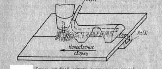
Next, the entire technological chain of operations for creating printed circuit boards (Fig. 3) and assembling printed circuit assemblies (Fig. 4) was reviewed, indicating the IPC standards that should be followed at each stage of production.
Rice. 3.
Scheme of construction of the PP manufacturing site
Scheme of construction of the PP manufacturing site (Fig. 3):
- CAD (receiving CAD data from the customer).
- CAM (processing of CAD data, preparation of control programs).
- New materials.
- Lead-free fiberglass laminates.
- FR4 with high Tg.
- FR4.
- Laying.
- Drilling.
- Applying a chemical coating of 2–3 microns.
- Layer-by-layer application.
- Laser plotter.
- Exposure.
- Removing PTEF.
- Manifestation.
- PTH output.
- Coating.
- Washing.
- Control.
- Electrolytic deposition of Cu 25 microns.
- Electrolytic deposition of Sn 4–5 µm.
- Removing photoresist.
- Copper etching.
- Removing metal resist Sn.
- IDF.
- Applying a solder mask.
- Exposure.
- Manifestation.
- Curing.
- Pickling and fluxing.
- HASL. or
- HASL SnPb, HSAL SnCu, ENIG, immersion Ag; Immersion immersion Sn, OSP.
- Water wash.
- Control.
- Printing of inscriptions.
- Wiring.
- Separation.
- Electrical testing.
- Manufactured products.
- Mechanical cleaning.
- Copper etching.
- Washing.
- Disposal.
Rice. 4.
Scheme of construction of the PU assembly section
Scheme of construction of the PU assembly section (Fig. 4):
- Pre-production (analysis of submitted projects).
- Solder paste.
- Stencils.
- Components.
- Dry storage cabinets.
- Printed circuit boards.
- Washing.
- Wave soldering.
- Hand soldering.
- Zaruzchik.
- Screen printing machine.
- Fuji is an automatic installer.
- Mydata is an automatic installer.
- Convection reflow oven.
- AOI (automatic optical inspection).
- Unloader.
- Zaruzchik.
- My 500 is a screen printing machine.
- Assembleone is an automatic installer.
- Mydata is an automatic installer.
- Condensation reflow furnace.
- Unloader.
- Repair center.
- X-ray control.
It should be noted that our foreign colleagues presented very clear and high-quality illustrative material showing the defects and the reasons for their occurrence. Examples were descriptions of defects that arise when incorrectly designing stencils for applying paste, selecting application parameters (Fig. 5) and temperature profile (Fig. 6).
Rice. 5.
Remains of paste after stencil application: a) large aperture; b) small aperture
Rice. 6.
The influence of the temperature profile on the formation of a solder joint: a) complete melting of the paste; b) incomplete melting of particles with a diameter of 0.25 mm; c) unfused particles with a diameter of 0.25 mm
High-resolution photographs of various defects were presented that can be detected visually (displacement of components, undercuts, voids and separation of solder joints, solder balls, poor wettability and some others), numerous microsections on which not only defects were visible (displacement of PP layers, rupture metallization of internal connections - between the inner layer and the wall of the hole and similar to those described above - Fig. 7, 8), but also the structure of the solder joint itself with intermetallic phases. The results of non-destructive types of testing were also presented - X-ray photographs (voids in solder joints, displacements of PP layers, splashes and balls of solder, etc. - Fig. 9, 10) and photographs taken on ultrasonic testing installations (delamination of microcircuits, lack of contact - Fig. 11, 12). Video materials were demonstrated: the process of soldering components and defects that occur when drying components (popcorn effect).
Rice. 7.
Crack in the inner layers of fiberglass
Rice. 8.
A crack inside the microcircuit (at the top is the microcircuit body, at the bottom is fiberglass)
Rice. 9.
An example of an X-ray image of a QFP chip, the defect is not soldered
Rice. 10.
An example of an X-ray image of a BGA chip, the defect is solder jumpers
Rice. eleven.
An example of ultrasonic testing of a board with microcircuits in BGA packages, areas of delamination are shown in red
Rice. 12.
An example of ultrasonic testing of a microcircuit in a SOIC 16 package, areas of delamination are shown in red
Questions about component coatings and board finish coatings, brands and types of soldering materials are considered, with a description of the most acceptable combinations and properties of coatings and materials.
Of particular interest was the discussion on the choice of board finish: comparative characteristics of coatings such as OSP (organic coating), HASL (hot tinning), ENIG (immersion gold), tin and silver were given. Comparative characteristics of finishing coatings are given: their shelf life, solderability, wettability and some other parameters (Fig. 13).
Rice. 13.
Example of solderability of various PP finish coatings
In addition to the well-known advantages and disadvantages of the listed finishing coatings, a very interesting topic was raised - replacing immersion gold with immersion silver. Our colleagues do not consider immersion gold to be the optimal coating (note that most domestic enterprises use either immersion gold or “good old” hot tinning). They pointed out such disadvantages of immersion gold as insufficient solderability (which can be caused by a poor-quality technological process - the mask is not completely etched) and the high rate of formation of intermetallic compounds with almost all metals included in the solder joint. At the same time, according to them, immersion silver does not have these disadvantages. A diagram of the process of silver deposition on copper was given with a description of the resulting coating characteristics (Fig. 14–17).
Rice. 14.
Technological chain of the process of forming the PP finishing coating: immersion silver ASIG
Rice. 16.
Autocatalytic silver deposition process: • Autocatalytic reaction, the deposition process is supported by a reducing agent in the electrolytic bath. • Creates a non-porous and very durable silver surface that blocks any diffusion of copper through the silver film during repeated reflow soldering or long-term storage.
Rice. 17.
Fine gold deposition process: • Due to autocatalytic silver deposition, the silver film is thick enough for further deposition of immersion gold. • Because of the small potential difference between gold and silver, and because silver is resistant to corrosion, it is possible to deposit a very thin layer of gold, resulting in significant cost savings compared to immersion gold.
The finishing coatings of the components themselves were also characterized (Table 1). In the following, we talked about the compatibility of component coatings and brands of soldering materials. Once again, the participants’ attention was focused on the need to take into account the moisture sensitivity of components, their storage and drying before installation. The video, which showed a steam-air explosion of a component in a BGA package, clearly demonstrated what can happen to a component that was not stored correctly and was not pre-dried. Another example showed how a component behaves in a QFP package: when installed on the paste and at the beginning of soldering, everything went fine, but when approaching the peak of the temperature profile (the paste had already melted), the component “rose” and then fell again - a solder joint was not formed, the reason for the defect is the same.
Table 1.
Comparative solderability characteristics of various component lead finishes
| Component Lead Coating | |||||||
| Sn-Pb | Sn-Bi | Sn-Cu | Sn-Ag | Sn-Pd-Au | Ni-Au | ||
| Alloy composition, % | Pb: 10 | Bi: 4 | Cu: 1.5 | Cu: 3.5 | – | – | |
| Melting point, °C | 183∼215 | 213∼227 | 227∼296 | 221 (eutectic) | Soluble coating | Soluble coating | |
| Solderability | Wetting | good | Will satisfy. | Weak | Weak | Will satisfy. | Weak |
| Soldering temperature, °C | good | Will satisfy. | Low | Low | Will satisfy. | Will satisfy. | |
| Connection strength | Will satisfy. | Will satisfy. | Will satisfy. | Will satisfy. | Will satisfy. | Will satisfy. | |
| Productivity | good | Will satisfy. | Will satisfy. | Low | Will satisfy. | Will satisfy. | |
| Cost/expenses | Optimal | Will satisfy. | Will satisfy. | Low | Low | Low | |
The brands of materials used during installation were characterized in terms of composition and compatibility with possible combinations of board finishes and components. In addition to the characteristics of the materials, statistical graphs were presented, for example, a graph characterizing the rate of dissolution of metals in tin-lead solder at 225 °C (Fig. 18).
Rice. 18.
Dissolution rate of metals in tin-lead solder at 225 °C
Possible combinations are considered: PP finishing coating – component lead coating – solder paste. The combination “lead-free paste – lead-containing component” was considered unacceptable, the best – “lead-containing paste – lead-containing component” and acceptable – “lead-containing paste – lead-free component”. At the same time, special attention was paid to components in packages such as BGA, CSP, QFN. The symposium participants received many questions about the possibility of soldering BGA microcircuits with lead-free pin coatings using lead-containing pastes, and what to do when using such components in special equipment. I would like to immediately note that neither Lars-Olaf Wallin, nor Lars-Gunnar Klang, nor their colleague who spoke the next day, Werner Engelmayer, could give precise recommendations for such a combination and guarantee the reliability of soldering.
The problem is that “mixed” (or “combined”) technology is used only in Russia. When a question was asked about soldering using mixed technology in military equipment, our foreign colleagues answered that such problems do not arise in their countries: soldering is carried out according to classical technology using exclusively lead-containing components. As a recommendation, it was proposed to use thermal profiles similar to lead-free technology in mixed technology, taking into account the heat capacity and complexity of the PU itself, thus, under the body of the BGA component there should be a temperature of ∼235 °C (Fig. 19). But even at this, they do not guarantee the reliability of soldering (further, in the review of Werner Engelmayer’s report, this issue will be covered in more detail).
Rice. 19.
Temperature change along the surface of the PU (under the microcircuit in a BGA package and on the chip of the microcircuit itself) during reflow soldering
The speakers focused on the problems of tin “whiskers” and “tin plague”. After all, as you know, it was the problem of the formation of tin “whiskers” that has led to more than one failure in critical components (for example, the failure of a nuclear power plant control unit and the failure of one of the satellites), the problem of the “tin plague” is not so widespread, but it also causes certain concerns. As for tin whiskers, our colleagues presented examples of these crystalline formations (Fig. 20). It should be clarified that according to their data, not only tin (Sn), but also zinc (Zn), cadmium (Cd), indium (In), lead (Pb), antimony (Sb), gold (Au) is prone to the formation of “whiskers”. ), aluminum (Al), silver (Ag, more precisely silver sulfide), but the question is the size of these crystalline formations: for tin they are most significant. Regarding the fight against “whiskers,” let’s quote the text from one of the slides: “At the moment, there is no theory that can predict the number or length of “whiskers” and the moment when their growth begins.” In domestic technology, it is believed that the addition of at least 5% lead suppresses the growth of “whiskers”, the length of which can lead to a short circuit.
Rice. 20.
Examples of a tin “whisker” defect (our colleagues have already divided them into 5 groups - knots, loops, threads, stripes and rings)
With the “tin plague” the situation is simpler: the occurrence of this defect is possible when using tin of high purity, about 99.99%. Thus, the addition of an impurity reliably guarantees the impossibility of the formation of “tin plague”. As an example, the following impurity values were given: >> 5% copper (Cu), or > 5% silver (Ag), or 0.5% bismuth (Bi), or 0.1% antimony (Sb), or 50– 100 ppm lead (Pb). Pictures of studies are presented showing the process of formation of α-Sn - “tin plague” (Fig. 21, 22).
Rice. 21.
“Tin plague”: a) samples made of tin with 0.5% copper at the beginning of the tests, after 1.5 and 1.8 years, respectively (samples were stored at a temperature of –18 ° C); b) cross section of a sample aged for 1.5 years
Rice. 22.
A sample of high purity tin (99.99%), which was stored at a temperature of –45 °C: a) the original sample; b) partial transition; c) complete transition
Conclusion: materials from foreign experts are of great interest and can be used in preparation for the release of PP and directly during their production. However, we have to admit that due to the “peculiarities” of the domestic industry, not all questions can be answered by our foreign colleagues.
The entire second day was devoted to Werner Engelmayer's report. Mr. Engelmayer is a recognized expert in the field of solder joint reliability. His report was extremely rich and informative. Thus, many graphs and diagrams were presented reflecting tests of solder joints for reliability, shear, coating wettability after accelerated aging, etc. These statistics are interesting and indicate that the most reliable are classic lead and lead-free soldering. Lead-free technology is under study. Mr. Engelmayer presented mathematical models of reliability criteria for solder joints (depending on many parameters, including taking into account the lead or non-lead component, its type, the total number of leads and their sizes, holding time and temperature during reflow, and many other parameters). However, this model is only applicable to classical lead technology.
This technique allows you to predict the reliability of a solder joint without testing (Table 2). Calculation of the total probability of system failure after N cycles is calculated using the formula:
where n i
— number
i
components;
β i
is the shape parameter of the Weibull distribution curve for solder joints
the i
-th surface mount component;
N i
,
j
is the number of cycles to which
the i
-th component is exposed at
the j
-th load level;
Nf ,
i
,
j
is the fatigue life of the solder joint of
the i
- th surface-mount component at
the j
-th load level to the total failure probability
x
%.
Table 2.
Calculation of system reliability (unreliable components whose design does not meet reliability requirements are highlighted in red: failure will occur within 2 months from the start of operation or during rejection)
| j | i | (cycles) | N f ( x %) (cycles) | N / Nf ( x % ) | FM (reliability) | |
| 1 | 1 | 144 000 | 12 200 | 0,146 | 2,42 | –0,00165 |
| 2 | 131 | 38 | 47,8 | 0,17 | –262000 | |
| 3 | 17 700 | 5160 | 0,352 | 1,62 | –0,00231 | |
| 1 | 1 | 31 600 | 2680 | 0,0037 | 14,06 | –0,000001 |
| 2 | 36 | 10 | 1 | 1,02 | –0,0501 | |
| 3 | 4410 | 1290 | 0,0078 | 9,84 | –5,6×10⁻¹⁰ |
Note.
The probability of system failure after 5 years of operation is FΣ(N) = 100%.
A model for lead-free soldering is currently being developed. When asked what to guide the mixed technology, Mr. Engelmayer replied that it is possible to take a double or triple margin in the assessment values; the model itself for lead-free soldering (in our understanding) is unlikely to be built - there are too many factors and combinations of parameters.
Numerous process parameters that affect solder joint quality and specific examples of possible defects were also presented, some of which are shown in Fig. 23–25. Including the defects we have already described (Fig. 26).
Rice. 23.
A defect in lead-free soldering is the rise of the fillet. (Common fillet lifting was first described in the NCMS and IDEALS programs.) • The cause of solder fillet lifting from the pad is believed to be low local melting temperature, which is due to lead contamination in Sn-xAg-yBi, not Sn-58Bi, lead-free solders. • Sn-Bi-Pb forms a phase with a melting point of 96 °C. • Upon additional research, this defect was also discovered in other lead-free solders, although not to such a strong extent.
Rice. 25.
Finishing coating PP immersion gold/brittle solder structure Finishing coating immersion gold with a “black pad” leading to almost complete brittle fracture along the boundary of the solder joint. This problem is associated with the high concentration of phosphorus at the Ni/intermetallic interface. It appears quite rarely. There are no high-quality diagnostic capabilities.
Note.
High-quality wetting occurred only along the crater-shaped “rim” of the site, where there was no coating at all or a small amount of it.
Rice. 26.
Tin “whiskers” on the terminals of the ceramic capacitor 0201
Components in BGA packages aroused increased interest among the symposium participants. The speaker presented a number of very interesting diagrams and illustrations of the voltages arising in the solder joint of the ball leads (Fig. 27).
Rice. 27.
Dependence of the deformation of the ball outlet on the deformation energy: a) total creep deformation after 2 thermal cycles; b) total creep strain after one temperature transition and 15 minutes of exposure
He characterized the defect of the ball output, which is called “head on a pillow” abroad (Fig. 28). The participants asked Mr. Engelmayer how the rebonding process (replacing or restoring ball pins) affects the reliability of a BGA chip. In his opinion, this process actually leads to the absolute irreparability of microcircuits. Most elements require no more than 3 re-solderings. Let's do the math: after installing the ball leads at the manufacturer (this procedure is usually forgotten and is not counted as a cycle), we preheat the chip to remove the balls and strip the substrate, the second cycle can be considered the process of restoring the balls itself - when we install the balls on the substrate, and the third cycle - soldering the microcircuit onto the board, thus we exhaust the life of the microcircuit by 100%. If you don’t just change the balls, but dismantle the microcircuit from the PU and restore it, then you get 5 cycles (plus two more cycles - installation and dismantling on the PU) plus installation of the balls at the manufacturer: there is no need to talk about reliability. In special equipment, rebonding is an undesirable process.
Rice. 28.
Head-on-pillow defect: caused by insufficient heating
Participants asked questions about the possibility of using mixed technology in special equipment. Based on his own experience, Mr. Engelmayer responded that he considered classical lead technology to be the best, lead-free technology and installation of lead-free components with lead-containing paste (we repeat, acceptable, but undesirable) and did not recommend the use of lead-containing components in lead-free technology. This point of view can be confirmed by numerous microsections showing the uneven formation of intermetallic compounds in the solder joint.
Data was also provided for components with leads under the component housing (Fig. 29). However, they are not yet so widespread in our industry; this information was more of an informative nature and did not raise a large number of questions. In addition to those indicated in the figure, a component with “column” leads was shown: this development makes it possible, through the use of refractory metal columns 2–3 mm long, to compensate for the difference in the LTLE of the PP and the component substrate.
Rice. 29.
Various pin types for surface mount components
Conclusion: at the moment, our colleagues from the IPC Reliability Committee have mathematical models and statistics on the behavior of solder joints using classical lead and lead-free technology; mixed technology is in the process of being reviewed and processed. The presented models can also be used with mixed technology by introducing a two to threefold reserve.
The third day of the symposium was the most interesting from the point of view of domestic technology: presentations were made by representatives of the leading enterprise of the industry, JSC Avangard, and the technical director of JSC OSTEK Enterprise, Stanislav Gaft.
The first part of the report was read by Nikolai Ivanov, Deputy General Director of Avangard OJSC for new equipment and technology. He demonstrated to the symposium participants a general test program for different modules using various components and soldering materials. The main goal is “comparative accelerated reliability testing of solder joints and identification of the most reliable solder joint designs from a large number of solder joint options, differing in geometric dimensions and various combinations of materials used, including component lead coatings, solder types and PCB pad finishes. The task of determining the lower limit of the average operating time of solder joints of various types is determined as a secondary result of comparative accelerated tests." This test program was agreed upon with the 22nd Central Research Institute.
The types of modules being tested and test devices created specifically for these studies that determine the presence of a circuit break (for example, ASR - an automatic recording stand) were presented. The elements used were “dummy” components of real components, in which the terminals located nearby are shorted in pairs, thus, using electrical control systems, our colleagues could clearly monitor the moments when a break occurred. A sharp jump in the circuit resistance was taken as a criterion for the occurrence of an open circuit; 10 such jumps were considered a defect, and the unit was rejected.
Using combinations of board finishes, components and soldering materials, a matrix of all possible combinations of these parameters was compiled. From all possible combinations, 128 variants of lead-free and combined solder joints and 2 exemplary ones (made using classical technology) were selected. 5 PUs were sealed using lead-free technology and 5 PUs using combined technology. PP with finishing coatings were used: OSP-Cu, chemical. Sn, HALS SnPb, HAL Pb-free, ENIG, ImSn, ImAg. Solder pastes POS61, Sn63Pb37 SAC305, Castin, Sn62 were used. Various ERIs were mounted: chip components in packages 01005-1206, ERIs in SOD80, SOT 23, SO8, BGA46T.75C, BGA169T1.5C, LQFP128T15.7, LQFP144T19.7, QFP100T25T, TQFP128T15.7, TSSOP28M25B, D packages IP8M3-TIN , DIP16M3F, D2PAK, TO220M3, HQFP48/64.8F, HSOP20M-F and some others with standard terminal finishes SnPb, Sn100, NiAu, NiPd, Sn97Bi3, SAC305, Sn98Cu2.
The tests themselves are divided into 2 groups: in one, slow impacts were carried out (40 test boards), and in the second, fast impacts were carried out (40 test boards). There was also a control batch of 20 test boards.
Vladimir Ivin, head of the radio-electronic technology department, reported on the test results. He demonstrated histograms of the distribution of failures by element after the first and second mechanical tests (multiple shocks, vibration): the bulk of failures occurred in chip components of standard size 0201, ERI in TSSOP, HSOP and TQFP packages. Regarding the combinations “finish coating of the board - component - soldering material”, the minimum level of defects (which was predictable) occurs with the classical technology; all other combinations resulted in a greater number of defects in one form or another. In addition to mechanical tests, the results of inspections after thermal shock were presented. Illustrations of specific defects were also provided.
Conclusion: the research conducted by Avangard OJSC is of great interest and has no analogues at the moment; these studies simulate real situations that are already taking place in real production facilities. Unfortunately, the tests have not yet been completed, but there is no doubt that, once carried out in full, they will be presented for discussion and as a guide to action for all enterprises involved in the production of special equipment.
After the representatives of Avangard, Stanislav Gaft, technical director of JSC OSTEK Enterprise, spoke. Since during the symposium the question of the optimal profile for soldering with mixed technology was repeatedly raised, he gave an example of calculation and construction of such. This information is useful for both experienced and novice technologists.
Outside the plan, the floor was given to Arkady Medvedev, President of the Guild of Professional Technologists, Honored Technologist of the Russian Federation, Professor of the Department of Instrument Engineering Technology at the Moscow Aviation Institute. Arkady Maksimovich once again called the imposition of lead-free technology a provocation of large companies producing mass electronics to suppress weak competitors. Lead in solders accounts for 0.05% of total lead use. In the first place are live bullets and batteries. Lead is widely used in cable sheathing, foundation waterproofing, paint and more. And no one is going to give it up for these types of uses.
However, for domestic production, one has to reckon with the inevitability of supplying components designed for lead-free soldering. National programs for the development of microelectronics technologies provide for the step-by-step integration of microcircuits up to a lithographic resolution of 45 nm, but do not plan chip packaging technologies. This means that we will again receive components from abroad with our chips, but in a lead-free version according to the Western version.
Arkady Maksimovich noted that against this background, R&D at Avangard OJSC is very relevant. This work is in demand in all branches of electronics in Russia. A large scope of work has been completed, worthy of all approval. The information they received is so broad and voluminous that after processing it, we will receive from them answers to all the questions that we need so much in our further work. Taking advantage of the presence of Nikolai Ivanov, Director of Science at Avangard OJSC, at the symposium, the President of the Guild of Professional Technologists expressed concern about the state of the program for updating the regulatory framework. JSC Avangard is the lead organization in the development of new standards. But there is still no analysis of the state of the issue, no standardization program, no consolidation of the efforts of leading experts in the development of new editions of standards, and most importantly, the concept in integration with the international system of standards has not yet been adopted. The procedure for harmonizing the standards being developed has not been determined. As a result, JSC TsNITI Tekhnomash has already released drafts of three documents that are in no way consistent with the international system of standards. Moreover, no one knows about their existence, there is no discussion of these editions. And the current standards are so outdated that they have become a brake on modern production. The Guild of Professional Technologists and the secretary of the technical committee TK91 (RKE-91) IEC K. N. Stas proposed concepts for options for the domestic standardization program, but did not receive an official response. As time goes on, enterprises are trying to solve their problems on their own using American IPC standards, which is not legitimate for critical electronics. And we are all waiting for the industry’s leading institute to become more active in this very important area.
Legislative initiative or trend of the times
Why is it now that lead-free solders have so quickly begun to gain ground over traditional compounds? The fact is that the EU Directive “On the Restriction of the Use of Hazardous Substances” (adopted in 2003 and entered into force on July 1, 2006) obliged to limit the use of lead (and five other substances) in the production of electrical and radio-electronic devices. This is due to the requirements of environmental safety and human health. Lead belongs to the group of heavy metals, and its vapors are highly toxic.
Although adherents of the usual POS-40 solder should not be upset. It is still produced and sold. In many countries, tin-lead solders are used in the transport, military and aerospace industries.
Features and main characteristics of lead-free solders
The main advantage of such compositions is absolute environmental safety. In addition, equipment and machinery manufactured with their use are much easier to dispose of.
The technological feature of these solders is their increased melting point. On average, it is 50 ⁰С higher than that of tin-lead analogues. This somewhat complicates the soldering process and increases the requirements for the equipment used.
According to the generally accepted classification, these compositions belong to soft solders. Tensile strength does not exceed 100 MPa.
It is impossible not to note such an important characteristic of these solders as high electrical conductivity.
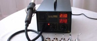
Soldering station, what kind of device is this?
A soldering station is special equipment designed for soldering. Absolutely any soldering station consists of a block and a soldering iron. This equipment is different from a simple soldering iron. Using a soldering station, you can not only perform soldering, but also remove excess solder. Sometimes this equipment functions as a hot air gun. And this is important. When working constantly, temperature control comes first. If this does not happen, then working with this tool will be impossible. Also, do not forget about the weight and size of this soldering tool. When transporting from place to place, this factor is quite significant. It is not always possible to work in one place. Therefore, too heavy and oversized devices cause a lot of problems when transporting a soldering station.
Soldering station with lead-free solders
As soon as the law came out, HAKKO immediately released “safe” equipment. But the company’s technologists have been working on developments in this vein since the early 90s. Many devices were created, many mistakes were made. But the work did not stop. And soon such a device appeared. Today, the company produces many such devices. And they are very in demand and popular. No other firms can compete with the Japanese company. Because HAKKO equipment works without interruption, is accessible and quite inexpensive. You can find this equipment on the shelves of specialized stores and online stores. There are few counterfeits in this area and the company carefully checks its products. In addition, the purchased product is given a certificate and a 5-year warranty. In the event of a breakdown, HAKKO provides repair or replacement of the purchased equipment.
The entire line of soldering stations with lead-free soldering tips differs from other tools in color. Soldering equipment with lead-free soldering tips is painted yellow-blue. They differ in that they are equipped with a powerful heating element (power from 75 to 160 W). This element is simply necessary. Without it, the soldering process simply will not happen. The melting point of lead-free solders reaches approximately 280-300 degrees. And to heat the place where the soldering process will take place, high power is needed. To avoid unpleasant moments when working with lead-free solder, it is best to use composite soldering heads.
Composite heads are a breakthrough in the field of soldering technology. To change the head you don’t need to put in a lot of effort and have the right tools at hand. it is not fixed by anything. You need to wait until the tool cools down or use a special heat-insulating grip and remove the head from the body of the soldering iron.
Installing a new head is also easy. No need to measure or use special tools. It doesn't matter at all how it will be located. The location of the head is important for the operator, as it is convenient for him to perform the work with it.
Composite soldering heads transfer heat better and with their help you can easily regulate the temperature, set exactly the temperature regime that is needed for the soldering process of a particular material. But recently, devices have appeared that automatically regulate the temperature. Each soldering head has its own personal barcode. When one or another head is connected, the computer analyzes the barcode and produces the desired temperature regime.
Health effects
The limited possibilities for using lead-free solders in electronics, their not very good wettability and unusual melting point cause dissatisfaction among many solders.
They question the safety of tin alloys. The opinion of some practitioners is that there are many inconveniences, but harm to humans still occurs.
The tin found in lead-free solders is toxic if particles enter the lungs. Tin boils at a temperature of 2600°. This is a very high figure, which, of course, is not achieved during the soldering process. Consequently, the release of tin vapor when soldering parts does not occur.
The metal itself is not dangerous. Tin is approved for use in the food industry. Therefore, the opinion about the toxicity of lead-free solders is not justified.
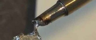
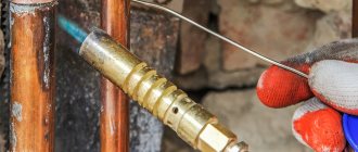
Soldering with lead-free solder is usually carried out according to a well-known scheme. The surface of the parts should be thoroughly cleaned, the selected solder should be melted, and distributed over the area to be soldered.
Particular attention should be paid to the heating temperature. Lead-free solders melt at lower temperatures
After cooling, you need to check the quality of the resulting connection.
Classification
- Lead-free solders are divided into several main types, the most commonly used ones can be considered.
- Copper is used as an additional element. This type of solder was created for soldering printed circuit boards. This is done using a wave of solder. However, if we draw parallels with other versions of lead-free solder, this one has a reduced strength property. This type also requires melting at a high temperature, which is not always required.
- Silver is used as an additional element. This type of tin solder, where lead in the chemical composition is replaced by silver, is the most commonly used relative to all other types. This modification lends itself well to soldering. In the deposited state, it has good strength properties and other mechanical characteristics. The substance begins to melt when it reaches two hundred and twenty degrees Celsius. This modification of lead-free solder in some cases can compete in characteristics with classic lead consumables.
- Tin solder with two additional chemical elements in the composition: silver and copper. This version of lead-free solder was the first to be used. It has a low melting point. A significant percentage, which takes values of ninety, is tin in the composition. Connections created using this subtype of lead-free solder have fairly high mechanical properties. This type, when compared with the two described above, is the best option from an economic point of view.
- Bismuth and silver are used as additional elements. This type, relative to all those described above, has the lowest melting point. This property significantly narrows the range of applications of this material. Of all the types of lead-free solders, this one is the best for soldering.
Copper-containing solders
Initially, a special solder Sn99/3Cu0.7 (with a copper content of 0.7%) was developed for automated wave soldering of printed circuit boards in factory conditions. The disadvantages of this composition include the relatively low mechanical strength of the joint. It is produced under the index POM-07 by the Russian Solder Plant (Novosibirsk). The most famous foreign manufacturers of this type of solder are Asahi (Singapore), Wyctin B&C (China) and Tamington (USA).
For soldering various products made of copper (especially drinking water pipes), brass, nickel, steel and alloys based on them, Sn97Cu3 solder (with a copper content of 3%) is used. Seams made using this composition have increased heat and cold resistance. The main suppliers of this type of solder on the Russian market are German manufacturers Rothenberger and Brazetec. Domestic manufacturers produce such products (St. Petersburg).
Types of tin solders, properties and characteristics
According to the chemical composition of the alloy, antimony solders, solders with a small amount of antimony (low-antimony), and alloys without antimony (antimony-free) are distinguished. All of the above types of solders are produced in accordance with GOST 21931-76 (in products), GOST 21930-76 (ingots).
There is another option for classifying tin solders. According to it, alloys are divided into:
— tin-lead (abbreviated POS);
- antimony (abbreviated POSSu);
— tin-lead-cadmium (abbreviated POSC);
- lead-free.
The latter are alloyed with copper, silver, zinc, aluminum, and cadmium.
POS tin solders (tin-lead alloys), having a tin percentage of 10% to 90%, are classified as soft solders.
They begin to melt at 183°C (the melting temperature of the tin-lead pair) and complete melting at different temperatures. This is determined by the chemical composition of the alloy. Namely:
POS-15 (tin 15%) - 280 °C.
POS-25 (25%) - 260 °C.
POS-35 (33%) - 247 °C.
POS-61, POS 63 (tin 61% and 63%) - 183 °C
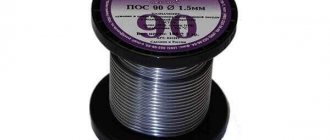
POS-90 (tin 90%) - 220 °C
Due to the fact that the composition of the POS-61 and POS-63 alloys is almost identical to the composition of the tin + lead eutectic, they melt at a constant temperature of 183 °C.
Soft tin solders also include:
— POSSu – used for soldering products made of zinc, galvanized metal, with high requirements for solder joints (antimony solders);
— OTs — for joining aluminum products (tin-zinc solders);
— POSK — for connecting products that react to overheating, piezoceramics, capacitor leads (tin-lead-cadmium);
- lead-free solders, which in addition to tin include silver, copper, bismuth and other metals.
Solder is an alloy consisting of low-melting metals. For example, tin. But soldering with tin alone is quite expensive. They work with pure tin only when it is necessary to obtain a junction that is absolutely harmless to humans: when soldering utensils for food consumption or medical equipment. In other cases, to reduce the cost of solder, cheaper but harmful lead is added to tin.
For reference: the surface of the solder is darker, the more lead it contains. A rod made of pure tin, when bent or compressed, produces a characteristic crunch.
The positive properties of tin solders include:
— strength combined with ductility;
— high thermal conductivity coefficient;
- corrosion resistance.
Tin solders are used to join parts made of almost all metals, and the more pure tin in the solder, the better the quality of the resulting connection. The advantage of PIC is its versatility. Soft solders are used in the form of sticks (rods); less often, wire or paste (a mixture of solder with a fluxing agent) is used. The more tin in the alloy, the stronger the connection between the parts when soldering.
This type of rolled tin is not used for soldering aluminum. Other metals, including copper and iron, lend themselves well to PIC soldering. The junction is the most vulnerable point of the metal-solder-metal connection. The strength of the solder depends on the chemical composition of the solder used. The tensile strength of the soldering area is 6-8 kg/mm2, increasing in proportion to the increase in the amount of tin.
Let's look at some features of using zinc and antimony as additives to solder when soldering certain metals. The addition of zinc when working with aluminum and alloys of this metal increases the corrosion resistance of the solder. Such CO solders, containing from 10% to 40% zinc, are used for ultrasonic or abrasive soldering and tinning.
When joining copper, adding antimony to the composition increases the strength of the joint. When soldering brass, antimony does not affect the strength of the joint. And iron reduces the strength of the joint.
Sometimes you can find a rod or wire for soldering without markings. The approximate chemical composition of such a product can be determined using the following parameters:
- a rod with a tin content above 60% shines brightly (perhaps it is POS-90, POS-61);
- material containing a lot of lead - dark gray, matte;
— a rod with a significant lead content is plastic (up to 60%), it is easy to deform (POS-40, POS-30);
- a rod with a lot of tin, strong and hard. It cannot be bent by hand;
— PIC of various brands melts at temperatures from 183 °C to 265 °C.
Features of soldering technology
The technology for producing work using solders that do not contain lead is practically no different from soldering with conventional components. However, some features should be taken into account.
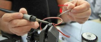
To the question of what they solder with, the answer is clear: a soldering iron. However, it is best to use a device with a thermostat. This will allow work to be carried out within the operating temperature range specified by the manufacturer. And it is significantly less than that of lead-based compounds.
To prevent overheating of parts and minimize thermal contact, it is necessary to select the optimal shape of the soldering iron tip. In addition, it should be borne in mind that a regular copper tip will not last long (when using such solders). It is better to use special tips coated with steel or coated with chrome and nickel.
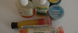
The choice of flux also plays an important role when working with lead-free solders. Usually, special compounds are used for this (usually more chemically active). The most convenient to use are liquids, gels and pastes that do not require subsequent cleaning of the soldering area.
Otherwise everything is as usual:
- heat the soldering iron to the required temperature;
- if necessary, clean the soldering areas;
- apply flux;
- simultaneously apply a solder rod and a soldering iron tip to the junction of the elements;
- let the soldered elements cool naturally.
The main problems encountered when soldering with lead-free solders.
Tin, without lead to tame it, behaves unpredictably. Tin plating without additives, like cadmium and zinc, spontaneously forms metal crystals about 1-5 microns in diameter and less than one-tenth the thickness of a human hair, which are pushed upward from the base. If they grow close enough to touch another conductive object, they will cause a short circuit that can damage the equipment. Thus, when working with lead-free solders, a number of problems arise that are associated with their physical properties. Let's look at the main problems that arise when soldering with lead-free solders:
- a higher melting temperature of soldering can damage electronic components containing plastic, and the components themselves can receive thermal “shock”;
— deformation of printed circuit boards may occur;
— weak moisture and spreading will be observed due to the increasing effect of surface oxidation;
— there will be a need to use more active (and corrosive) fluxes;
— the appearance of jumpers and short circuits is possible;
— due to the higher soldering temperature, strong spattering of flux will be observed;
— the time for creating high-quality soldering (contact) will increase;
- the appearance of the soldered contact will be duller;
— the lifespan of normal operation of soldering heads will decrease;
— it will be necessary to change the style of work of installers.
So, jumpers and short circuits may appear, and strong flux splashing may occur. Jumpers and shorts appear in the form of tin “whiskers” (these are microscopic sprouts of metal from solder joints on a printed circuit board). These mysterious seedlings were responsible for serious electronic failures. The proposed safe silver-tin-copper (SAC) solder only slows down, but does not stop, the growth of whiskers. But SAC solder has a greater environmental impact than the tin-lead option. Reliable lead-free technologies are likely to be available soon, although experts doubt it (companies like IBM and National Instruments are said to now have RoHS-compliant technologies even for lead-exempt products, but this expert debate goes like this , as if it remains open, and so far the most recent reliable source of information on this issue is the manufacturers of electronics products).
How to avoid defects when repairing computer equipment when manually soldering components made using lead-free technology? Large integrated circuit manufacturing companies - Texas Instruments, AMD, Fairchild Semiconductor, Philips and many others are completely switching to lead-free technologies. Manufacturers of discrete semiconductors and passive components (ON Semiconductors, Vishay, Samsung Electr-Mechanic) will do the same. Components made using traditional technology will be available only on order. In this regard, the use of lead-free components in all products is a matter of near future for all electronics manufacturers. In the foreseeable future, this problem will sooner or later affect everyone else.
There is an argument that lead-free components require special hand soldering techniques. This point of view is also common among developers, electronic equipment manufacturers and repair specialists. All leading manufacturers are unanimous that most Pb-free components are fully compatible with standard hand-soldering technologies using tin-lead solders.
Compatibility with RoHS requirements, as well as the “Pb-free” mark, does not mean that the element must be soldered with lead-free solder. But during the soldering process, it is necessary to prevent thermal destruction of electronic components (this trouble can arise because most of the “Pb-free” solders have an elevated melting point, which is incompatible with the maximum soldering temperature of the selected components). Experts in soldering technologies and soldering equipment claim that if you follow a number of recommendations for manual soldering (see below), the quality of soldering and components of electronic circuits will not be affected.
For hand soldering, it is necessary to select soldering stations that have sufficient power reserves, thermal stability and the ability to maintain constant temperatures when operating at higher levels required for lead-free materials. Since lead-free solder has a higher melting point than lead-containing solder, the tip temperature should be approximately 343°C (lead solder required 315°C). In this mode, the durability of traditional soldering tips is sharply reduced and therefore, during the soldering process, it is necessary to use nozzles designed specifically for “Pb-free” soldering. Modern soldering stations provide the above requirements, but when working with lead-free solders, in order to maintain the required temperature profiles of some components, it makes sense to quickly remove the tip from the soldering site. The wettability of lead-free materials is worse than that of lead-containing materials. In addition, they have worse oxidation during soldering, the formation of crystalline threads is observed, etc. It is known that the fewer oxides, the easier the soldering process is, therefore soldering is often used in a nitrogen environment or special fluxes are used. Nitrogen, being an inert gas, protects metal surfaces heated during soldering from oxidation. In this case, the requirements for flux are not categorical, wettability increases, solders are easier to work with, and the quality of joints improves. When manual soldering in conditions of non-serial production, the task of removing oxides and ensuring the spreadability of solder is no less performed by flux. This is a serious alternative to soldering in a nitrogen environment. During the soldering process, it is necessary to monitor the condition of the soldering station tip to avoid its oxidation.
If "Pb-free" solder is used, it should be cleaned more thoroughly and kept completely covered with solder at all times. When working with “Pb-free” components, their installation and disassembly, on a board of mixed type, it is necessary to thoroughly clean the component seats in order to avoid mixing “Pb-free” and traditional solders, since failure to comply with this recommendation will result in “ cold soldering.
The use of desoldering pumps, braids for removing solder, etc. is becoming more relevant. Also, following the above point, you should use different tips for soldering “Pb-free” and lead-containing solders. With microcircuits in BGA packages, work is more difficult, but the situation is “saved” by products that produce modernized infrared soldering centers. When working with “Pb-free” solders and BGA microcircuits, the advantages of such soldering centers are undeniable. They have unsurpassed uniformity of local infrared heating, which ensures accurate and safe (for sensitive components) thermal profile processing. Soldering centers provide the ability to visually monitor the soldering process (an additional option is a video system). Such a system is universal and self-sufficient; it ensures reliable and safe work with complex-profile components.
Three-component solders
What are electrical parts and radio components used for soldering today at modern enterprises (as well as numerous DIY enthusiasts)? Three-component SnAgCu solders. It is this composition that combines all the advantages of lead-free products, has good performance indicators, a low melting point (217 ⁰C) and an optimal price/quality ratio.
The scientific debate about the ratio of components has been going on for quite some time. Today, the optimal content (both according to manufacturers and reviews from numerous consumers) in such solder is considered to be 95.5% tin, 3.8% silver and 0.7% copper (Sn95/5Ag3/8Cu0.7). It is widely used in enterprises producing electronic equipment and electrical equipment. In addition, it is quite easy to work with it at home. Such solders cope quite successfully with old, heavily oxidized parts. In Russia, the most popular products are those of the famous German manufacturer Stannol.
Solder balls
Solder balls on the surface of the printed circuit board indicate that the liquid fractions of the flux have not evaporated before wave soldering of the product. Typically, such balls appear when the operator first works with water-based flux (VOC free). Solder balls splash onto the surface of the board through the mounting holes as the flux boils. Microscopic balls indicate the need to increase the duration or temperature of preheating the board so that the solvent included in the flux has time to completely evaporate.
The appearance of solder balls on the underside of the board may be due to insufficient flux solids. Increasing the solids content reduces the number of such balls. However, solder balls on the bottom surface of the board are more often caused by the solder mask. Solder sticks either because the solder mask softens or because the solder mask becomes too smooth. To eliminate this defect, check the mask material or solder the circuit assembly with a lower preheat temperature and/or solder bath temperature.
Lead-free solders and their properties
Replacing traditional types of solders with lead-free materials is not only the spirit of the times, but also a requirement of numerous international environmental commissions. The article examines the properties of various types of lead-free solders and provides recommendations for their use.
PDF version (909Kb)
Among the thermal, mechanical, fatigue and other properties of solders, one of the most important is the melting point. Table 1 shows some of the commonly known types of lead-free solders [1].
It should be noted that work continues to optimize the compositions of lead-free solders to achieve the required properties. For this reason, the compositions of the solders shown in Table 1 may from time to time differ slightly from commercially produced solders. For example, Table 2 shows the brand names of some commercially available solders from various manufacturers.
Lead-free solders with high indium content (such as the first solder in Table 2) are inherently incompatible with indium and lead materials, regardless of whether the latter is present on the surface of the printed circuit board or on component leads. To achieve a completely lead-free process, in some cases (for example, when using alloys containing indium), it is necessary to use a lead-free coating of solder surfaces of printed circuit boards and component leads.
Table 1. Examples of some lead-free solders and their properties [1]
| Lead-free composition | Temperature | Notes |
| solder | melting point, °С | |
| 48 Sn/52 In | 118(eutectic | Low melting point, high |
| temperature) | cost, low strength | |
| 42 Sn/58 Bi | 138(eutectic | Standard, availability depends |
| temperature) | availability of bismuth | |
| 91Sn/9Zn | 199 (eutectic | High degree of slag formation, |
| temperature) | corrosion resistance | |
| 93.5Sn/3Sb/2Bi/1.5Cu | 218(eutectic | High strength, high |
| temperature) | resistance to thermal fatigue | |
| 95.5Sn/3.5Ag/1Zn | 218…221 | High strength, good |
| resistance to thermal fatigue | ||
| 99.3 Sn/0.7 Cu | 227 | High strength, high temperature |
| melting | ||
| 95 Sn/5 Sb | 232…240 | High shear strength, |
| resistance to thermal fatigue | ||
| 65Sn/25Ag/10Sb | 233 | Motorola Patent, High Durability |
| 97Sn/2Cu/0.8Sb/0.2Ag | 226…228 | High melting point |
| 96.5Sn/3.5Ag | 221 (eutectic | High strength and high |
| temperature) | melting temperature |
From Table 1 it can be seen that lead-free solders are characterized by either too low or too high melting points compared to eutectic lead-based solders.
tin solders. Table 2 lists mainly lead-free solders with high melting points.
When using low-temperature solders, a special flux is required, since standard flux is inactive at low temperatures. Another limitation associated with low temperature solders is the reduction in their wetting properties caused by reduced fluidity at subeutectic temperatures.
For low temperature applications, solders containing indium have gained some acceptance. Thus, many companies use solder containing 52% 1p and 48% BP, since it provides better performance when re-soldering during repair or rework. Because this solder has a melting point of 244°P (118°C), re-soldering at a lower temperature can be done many times without risk of thermal damage. If the printed circuit lines of the board are coated with gold as an antioxidant, then using indium solder prevents leaching of gold [2].
Another lead-free solder with a low melting point is 42 Bp/58 B solder. If you look at the phase diagram of solder BnY, you can see that the melting temperature is at
level 138°C. Bismuth is used in solder alloys to achieve low melting temperatures, but bismuth-containing alloys generally have poor wetting characteristics.
Many of the other alloys shown in Table 1 have a higher melting point than the lead-tin eutectic alloy, which has a melting point of 183°C. This is, for example, zinc-tin high-temperature lead-free solder with a melting point of 198°C.
High temperature solders are not compatible with commonly used printed circuit board materials such as RI-4. Additionally, higher re-soldering temperatures may increase the risk of board damage.
There are currently no lead-free solders that completely replace lead-containing solders, although some manufacturers describe their solders as “almost identical” [3]. Even in this case, re-soldering requires a soldering iron tip temperature of 400°C. For some applications, this temperature may be too high and cause thermal damage.
One of the key problems with using high-temperature solders, presented in Tables 1 and 2 when wave soldering, is the increased risk of capacitor breakdown. When wave soldering, the temperature should be maintained in the range of 230...245°C, which is 45...65°C higher than the melting point of tin-lead solder. Lead-free solder with a melting point of 220°C will require a temperature of 265…280°C during wave soldering. This increases the temperature difference between preheating and wave soldering and therefore increases the risk of damage to the capacitors.
In general, almost all lead-free solders have lower wettability (flowability) than eutectic tin-lead solders, and therefore the former fill the required area less well. To improve fluidity, special flux compositions are required. The fatigue characteristics of lead-free solders are also not good enough, although in one
Table 2. Examples of lead-free solders from various manufacturers (courtesy of Dr. Raiyoman Aspandiar, Intel Corporation)
| Solder type | Provider | Compound | Melting point, °C | Notes |
| Incompatibility of indium and lead. | ||||
| Indalloy™ 227 | Arconium Specialty Alloy | 77.2 Sn/20 In/2.8 Ag | 187 | Requires lead-free coating of PCB pads and IC pins Temperature too high |
| Alloy H™ | Alpha Metals | 84.5 Sn/7.5 Bi/5 Cu/2 Ag | 212 | liquidus. When wave soldering, a temperature of more than 260-C is required Incompatibility of indium and lead. |
| Tin-Zinc Indium | AT&T | 81 Sn/9Zn/10ln | 178 | Lead free coating required |
| contact pads of the printed circuit board and microcircuit pins | ||||
| Castin™ | AIM Products US Dept. of Energy (DOE) | 96.2 Sn/2.5 Ag 0.8 Cu/0.5 Sb | 215 | Liquidus temperature too high. When soldering with wave |
| Tin-Silver-Copper | (US Department of Energy) | 93.6Sn/4.7Ag/1.7Cu | 217 | requires a temperature of more than 260-C |
From the studies, no failure of solder joint integrity was observed after thermal cycling testing for 96.5 Bp/3.5 Ag high-temperature solder (the last alloy in Table 1) [4].
Ideally, the melting temperature of the selected solder should be about 180°C, so that a temperature of 210...230°C is used for reflow; for wave soldering - 235...245°C, and for manual soldering - 345...400°C. Higher hand soldering temperatures should only be used by highly qualified
installers to avoid thermal damage.
IPC specification J-STD-006 provides a detailed list of tin-lead and lead-free solders. However, none of the lead-free solders are considered a complete replacement for eutectic tin-lead. Currently, research is underway to develop lead-free solder, which will become a full replacement for the above-mentioned tin-lead solder. This is an urgent requirement that must inevitably be taken into account.
Literature
1. Sokolowski, Norbert. Lead free alloys and limitations for surface mount assembly. Proceedings of Surface Mount International, 1995, pp. 477-480.
2. Keeler, R. Specialty solders outshine tin/lead in problem areas. EP&P, July 1987, pp. 45-47.
3. Seelig, Karl. A study of lead free solder alloys. Circuit Assembly, October 1995, pp. 46 - 48.
4. Melton, Cindy. How good are lead free soldiers. SMT, June 1995, pp. 32-36.
The article was prepared using materials from the site www.rayprasad.com