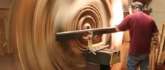
Step by step process
Each stage contains detailed comments and photographs with examples.
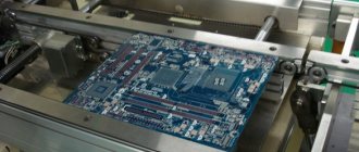
Printing tracks on paper
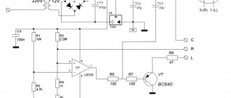
Open the board diagram. The article uses the Sprint-Layout program and a transistor multivibrator circuit.
Printing a diagram on paper
Use as much printing space as possible so you don't have to reprint the design again and have spare stencils ready.
There is no need to mirror the board if it was drawn from the radio components side. We also remove macros and other layers, we only need the tracks and the board border.
The quality of the transferred tracks onto the textolite also depends on the type of paper chosen.
There are several options:
- Plain paper;
- Glossy paper. Can be used from any magazine;
- Self-adhesive wallpaper backing. Excellent transfer of tons to textolite;
- Soft coated paper. This one is sold on Aliexpress.
Thick A4 office paper for LUT. The toner comes off worse.
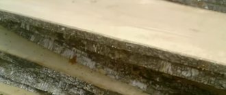
An example of an unsuccessful transfer of a board to PCB. Half the tracks are missing.
Example of a bad transfer
You can actually make printed circuit boards using office paper, but you need a good printer and toner. Such paper is capricious, and if you do not heat it well, or overheat the board, then nothing will work.
Glossy differs from office thickness. Its disadvantage is that it gets stuck in the printer during printing. Glossy paper also tears easily and is easier to overheat than office paper.
Self-adhesive paper backing and printed circuit boards
Self-adhesive wallpaper backing has gained popularity among radio amateurs. It quickly transfers toner to the PCB, but it is also quite difficult to print a printed circuit board on it.
We are talking about a soft surface from which self-adhesive wallpaper can be removed. Also, such a substrate sometimes gets stuck in the printer during printing.
It doesn't make much sense to cut out an entire A4 format from such wallpaper. In this format, the paper will slip out from under the drum during printing. Use small pieces of backing so you can stick them to plain paper.
Do not use liquid glue or other liquid materials. You may damage the drum unit during printing and leave marks on it. You can also glue it with the wallpaper itself.
Soft coated paper is sold on Aliexpress. It is yellow. Similar to glossy paper, it jams in the printer. It all depends on your printer model.
Printing and preparation
You can cut the PCB using a hacksaw, scissors or cutting discs.
Preparation and marking of textolite
We cut off the board with a margin to make it more convenient to apply the tracks while heating with an iron.
We use velvet sandpaper to treat the surface of the textolite. We clean it from dirt and copper microparticles with acetone or isopropanol.
Drawing tracks
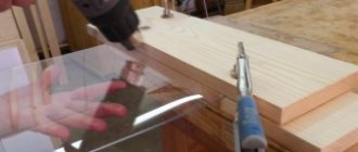
You will need an iron, a board, paper and a container of water.
We heat the iron to 100 °C and place the textolite on a wooden board. Why wooden? It heats up quickly and slowly releases heat to the environment.
We place the heated iron on the textolite. Hold for 20 seconds. The hot PCB will grab the paper.
We warm the textolite
Place the stencil on the heated textolite. It partially sticks.
Place one sheet of paper on the PCB and iron the board for one or two minutes. Paper is needed to reduce overheating. Ironing should be done carefully, without sudden movements.
Drawing tracks
Leave the board to cool for five minutes so that the toner does not come off the copper. Place it in a container with water.
Removing paper from the board
We also wait about five minutes. Using your fingers or a sponge, remove the layer of paper.
Never remove the paper with your fingernails. This can remove the toner from the copper.
Removing borders on the board. They are not needed from the side of the tracks.
Restoring contacts
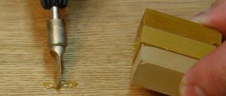
The tracks can be restored with a perforated marker or nail polish. Apply varnish or marker to the damaged area.
Restoring tracks with nail polish
This will protect the copper during solution etching. Wait until the varnish is completely dry so that it is resistant to water.
Everything is ready for the next stage.
Board etching
Basic and popular methods:
- Ferric chloride. Can be reused. If handled carelessly, it leaves marks on clothing and skin;
- Copper sulfate. Sold in gardening stores. Etches the board slowly;
- Hydrochloric acid. A fast and dangerous option. In addition, acid is difficult to obtain. Releases dangerous toxins;
- Electrolysis. The longest and least effective method;
- Hydrogen peroxide. Affordable and effective solution. The main disadvantage is that it cannot be reused. During etching, deposits form, which slow down the etching rate.
Etching Components
In this article we will use the peroxide method. For a board with an area of 100 cm, 100 milliliters of 3% hydrogen, 30 grams of citric acid and 5 grams of table salt are enough.
The etching process begins.
In a plastic container, mix all the components until completely dissolved, and place the board in the solution.
Etching process
Printed circuit boards should be etched in a ventilated area. When etching, toxic copper fumes are released.
To prevent the etching process from slowing down, stir the solution.
How to speed up etching
To increase the speed of copper etching, it is necessary to heat the solution. It is a catalyst for a chemical reaction.
Use a cotton swab to mix the solution for better etching.
Heating the solution using a second container
There is no need to pour boiling water into the solution itself. Pour boiling water into another container and place the container with the solution on it.
Small patches of copper remain
After etching, rinse the board in cold water and leave to dry. The etching solution can be poured into the sink like regular waste.
Drilling
You can drill holes both before and after etching. A screwdriver or drill is suitable as a tool.
Before drilling the board, it is advisable to core the holes. These are recesses for precise positioning of the drill. If you don't have a core, you can use a nail.
Do not make too large recesses and do not take nails with a larger diameter than the future hole on the board.
The main disadvantage of screwdrivers is their low speed.
The smaller the diameter of the drill, the faster the revolutions should be.
A screwdriver will not be able to make holes with a diameter of less than 0.8 millimeters. At low speeds, the drill will quickly become dull. If you put too much pressure on the drill from above, it will bend or break.
The drill's speed reaches 10,000 per minute. Therefore, for holes smaller than 0.8 millimeters it is better to use it.
Install the drill into the collet.
Center the drill and secure it.
Wear protective clear glasses during this type of work. Sawdust can get on your face from high speeds. Wear a dust mask.
You need to drill on the board and only perpendicular to the board. If the angle is sharp or you hold the board in your hands, the drill will fly out or break.
Next, we clean the board with sandpaper to remove burrs and pieces of PCB. We remove excess pieces of the board and form the border using macros.
How to Apply Macros
Macros are pictures on the printed circuit board that are located on the reverse side. And they can be applied in the same way as tracks on the board. Only now you need to mirror the macros, and then they can be applied to the back of the board.
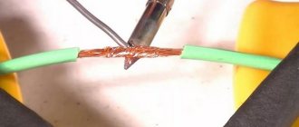
Soldering and checking operation
Clean the printed circuit board with velvet sandpaper. Tin the tracks using alcohol rosin. No need to use soldering acid.
Fully assembled circuit
First in line are small radio components. Solder them first. Transistors and LEDs are sensitive to temperature, so they must be soldered carefully and intermittently.
Ready multivibrator
After soldering, we check the operation of the circuit. Check the board for metal debris. The multivibrator can be connected to a regular battery with a voltage of 4 volts.
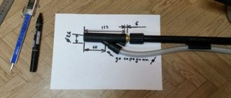
034-Tinning of the printed circuit board with Rose alloy.
After etching and clearing the printed circuit board of toner, it must be removed. This must be done in order to prevent the copper of the tracks from oxidizing. It is impossible to solder anything normally onto oxidized tracks - the solder will not stick. Another reason is improvements in the quality of the tracks. LUT is not capable of providing an ideal track quality. Due to the fact that the toner does not lie completely tightly, the tracks may be etched during etching. As a result, holes in the copper layer are visible in the light. This is especially true when etching a board with a thin layer of copper. Well, there is another reason - the tinned board becomes visually more attractive (it becomes pleasant to work with it yourself :)). You can tin the board with regular solder using a soldering iron. To do this, you need to wrap the soldering iron tip with a braid and, having collected solder into the braid, walk along the paths of the board, after moistening them with flux (alcohol-rosin, for example). This method has a number of disadvantages: the tracks overheat once again; the layer turns out uneven (critical when using SMD components); The appearance of such a board leaves much to be desired.
An alternative is tinning with Rose alloy . Rose's alloy is an alloy of various metals (Tin 25% / Lead 25% / Bismuth 50%) which has a melting point of only 94°C. Rose alloy melts in boiling water. This is where we will tin our board.
Let's start with the materials.
We'll need Rose's alloy. You can find it in radio stores, on the radio market, or order it on the Internet (that's what I do). You don’t need to buy a lot - it is consumed economically (50 grams of alloy will last you a long time). You also need a little food-grade citric acid, it will act as a degreaser-flux.
Tools needed:
A piece of non-foil PCB (about the size of our board) and a rubber spatula. We will tin the board with a rubber spatula. Does it sound strange? But it’s convenient! The spatula needs to be trimmed a little so that it is smaller - it’s more convenient.
How to tin a printed circuit board with Rose alloy.
1 Pour water into an enamel or aluminum container. The bottom of the container should be flat. Add a teaspoon of citric acid. Bring the water to a boil.
2 Next we throw a small piece of alloy into the water. You don't need a lot - one tablet is enough :). We are waiting for it to melt.
3 After the alloy has melted, we throw the board. The board tracks, under the influence of citric acid, will turn pink and the alloy easily sticks to them. Using a spatula, you need to “smear” the tracks on both sides of the board with the alloy. Take tweezers or something else to make it easier to twirl the board.
4 Next, you need to place a piece of PCB without foil under the board and carefully “clean off” the excess alloy from the tracks with a spatula. Without a PCB backing, the scraped alloy will stick to the bottom layer (if the board is single-sided, you don’t have to put a backing on it).
5 We take out the board, rinse it with water, wipe it with a handkerchief - you're done!
Finally, a comparison of the paths “in the light” before and after tinning.
It can be seen that after tinning the paths became much better, there were fewer “holes”. The aesthetics of the board have improved; soldering on it will be a pleasure.
PS Wood's alloy is also used for tinning boards.
But I don't recommend you use it. Firstly, its melting point is lower, and secondly, it is more harmful. (Visited 21,338 times, 1 visits today)
Errors during production
Common mistakes include overheating the board and poor etching solution. Always mix all the components of the solution, otherwise it will not begin to etch the board. Soldering acid should not be used when tinning the board. It will damage the board over time if you don't clean it well.
Some radio amateurs also have the practice of tinning boards with Rose alloy. You should not do this, since such an alloy is intended for desoldering parts, and not for permanent soldering. In addition, it is fragile and will quickly oxidize over time.
other methods
You can also make a printed circuit board using photoresist, but this method is more complicated and more expensive than LUT. There is also the option to order a printed circuit board online, but you will have to wait two weeks for it. And the price may be higher, and it will not be possible to quickly fix the error on the board.
You can also assemble the board using circuit boards (breadboards).
Breadboard example
Technology of applying a printed circuit board pattern using a laser printer
When printing on a laser printer, the image formed by the toner is transferred, due to electrostatics, from the photo drum on which the laser beam drew the image, onto paper. The toner is held onto the paper, preserving the image, only due to electrostatics. To fix the toner, the paper is rolled between rollers, one of which is a thermal oven heated to a temperature of 180-220°C. The toner melts and penetrates the paper texture. Once cooled, the toner hardens and adheres firmly to the paper. If the paper is heated again to 180-220°C, the toner will again become liquid. This property of toner is used to transfer images of current-carrying tracks onto a printed circuit board at home.
After the file with the printed circuit board design is ready, you need to print it using a laser printer onto paper. Please note that the image of the printed circuit board drawing for this technology must be viewed from the side where the parts are installed!
An inkjet printer is not suitable for these purposes, as it works on a different principle.
Preparing a paper template for transferring the design to the printed circuit board
If you print a printed circuit board design on ordinary paper for office equipment, then due to its porous structure, the toner will penetrate deeply into the body of the paper and when the toner is transferred to the printed circuit board, most of it will remain in the paper. In addition, there will be difficulties in removing paper from the printed circuit board. You will have to soak it in water for a long time. Therefore, to prepare a photomask, you need paper that does not have a porous structure, for example, photo paper, backing from self-adhesive films and labels, tracing paper, pages from glossy magazines.
I use old stock tracing paper as the paper for printing the PCB design. Tracing paper is very thin and it is impossible to print a template directly on it; it gets jammed in the printer. To solve this problem, before printing, you need to apply a drop of any glue to a piece of tracing paper of the required size in the corners and glue it to a sheet of A4 office paper.
This technique allows you to print a printed circuit board design even on the thinnest paper or film. In order for the toner thickness of the drawing to be maximum, before printing, you need to configure the “Printer Properties” by turning off the economical printing mode, and if this function is not available, then select the coarsest type of paper, for example cardboard or something similar. It’s entirely possible that you won’t get a good print the first time, and you’ll have to experiment a little to find the best print mode for your laser printer. In the resulting print of the design, the tracks and contact pads of the printed circuit board must be dense without gaps or smudging, since retouching at this technological stage is useless.
All that remains is to cut the tracing paper along the contour and the template for making the printed circuit board will be ready and you can proceed to the next step, transferring the image onto fiberglass laminate.
Transferring a design from paper to fiberglass
Transferring the printed circuit board design is the most critical step. The essence of the technology is simple: paper, with the side of the printed pattern of the tracks of the printed circuit board, is applied to the copper foil of fiberglass and pressed with great force. Next, this sandwich is heated to a temperature of 180-220°C and then cooled to room temperature. The paper is torn off, and the design remains on the printed circuit board.
Some craftsmen suggest transferring a design from paper to a printed circuit board using an electric iron. I tried this method, but the result was unstable. It is difficult to simultaneously ensure that the toner is heated to the required temperature and that the paper is pressed evenly onto the entire surface of the printed circuit board when the toner hardens. As a result, the pattern is not completely transferred and gaps remain in the pattern of the printed circuit board tracks. Perhaps the iron was not heating up enough, although the regulator was set to maximum iron heating. I didn’t want to open the iron and reconfigure the thermostat. Therefore, I used another technology, less labor-intensive and providing one hundred percent results.
On a piece of foil fiberglass laminate cut to the size of the printed circuit board and degreased with acetone, I glued tracing paper with a pattern printed on it in the corners. On top of the tracing paper I placed, for more even pressure, heels of sheets of office paper. The resulting package was placed on a sheet of plywood and covered on top with a sheet of the same size. This entire sandwich was clamped with maximum force in clamps.
All that remains is to heat the prepared sandwich to a temperature of 200°C and cool. An electric oven with a temperature controller is ideal for heating. It is enough to place the created structure in a cabinet, wait for the set temperature to reach, and after half an hour remove the board to cool.
If you don’t have an electric oven, you can use a gas oven by adjusting the temperature using the gas supply knob using the built-in thermometer. If there is no thermometer or it is faulty, then women can help; the position of the control knob at which pies are baked is suitable.
Since the ends of the plywood were warped, I clamped them with additional clamps just in case. To avoid this phenomenon, it is better to clamp the printed circuit board between metal sheets 5-6 mm thick. You can drill holes in their corners and clamp printed circuit boards, tighten the plates using screws and nuts. M10 will be enough.
After half an hour, the structure has cooled enough for the toner to harden, and the board can be removed. At the first glance at the removed printed circuit board, it becomes clear that the toner transferred from tracing paper to the board perfectly. The tracing paper fit tightly and evenly along the lines of the printed tracks, rings of contact pads and marking letters.
The tracing paper easily came off from almost all the traces of the printed circuit board; the remaining tracing paper was removed with a damp cloth. But still, there were gaps in several places on the printed tracks. This can happen as a result of uneven printing from the printer or remaining dirt or corrosion on the fiberglass foil. Gaps can be painted over with any waterproof paint, manicure polish, or retouched with a marker.
To check the suitability of a marker for retouching a printed circuit board, you need to draw lines on paper with it and moisten the paper with water. If the lines do not blur, then the retouching marker is suitable.
It is best to etch a printed circuit board at home in a solution of ferric chloride or hydrogen peroxide with citric acid. After etching, toner can be easily removed from the printed tracks with a swab soaked in acetone.
Then holes are drilled, conductive paths and contact pads are tinned, and radioelements are sealed.
This is the appearance of the printed circuit board with radio components installed on it. The result is a power supply and switching unit for an electronic system that complements an ordinary toilet with a bidet function.