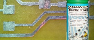
Copper plating solution for chemical plating
In this article I will tell you how to properly prepare a solution of chemical copper plating, which is one of the stages of metallization of holes in printed circuit boards.
Preparation of chemical metallization solution
To prepare the solution you will need inexpensive reagents. They can be bought in online stores, of which there are now many and they work with individuals. There should be no difficulties with the acquisition, if there is a desire.
The composition of the solution is as follows:
CuS04*5H2O (copper sulfate) - 30 g. NiCL2*6H2O (nickel chloride) - 4 g. NaOH (sodium hydroxide, caustic soda) - 50 g. Na2CO3 (sodium carbonate, soda ash) - 20 g. Trilon B - 85 gr. K3[Fe(CN)6] (potassium iron sulfide, red blood salt) - 0.1 g. KNCS (potassium thiocyanate) - 0.003 g. Formalin 20 ml/l. Distilled water - 1 l.
Order of mixing reagents
1. We weigh 30 grams. - copper sulfate and 4 g. - nickel chloride. Pour 0.4 liters of distilled water into a container and dissolve these reagents in it.
2. We weigh 50 grams. - caustic soda, 20 gr. - soda ash and 85 g. — trilona B.
3. Pour 0.4 liters of water into another container and dissolve the reagents in the following sequence.
First caustic soda, then soda ash and last Trilon B.
4. We mix these solutions by pouring a solution of copper sulfate with nickel into a solution with Trilon B, soda and caustic soda. Mix well and bring the volume of the solution to 1 liter with water. Let it stand for 5..10 minutes, if there is a slight sediment, then filter the solution.
5. Weigh 1 gram. potassium iron sulfide (red blood salt), dissolve it in 100 ml. distilled water. Then we take 10 cubes of this solution with a syringe - this will be 0.1 g. this reagent and add it to the just prepared chemical solution. copper plating
6. Weigh 1 gram. potassium rhodanate and dissolve it in 100 ml. distilled water. Then we take 0.3 cubes of this solution with a syringe - this will be 0.003 g. and also add it to the main solution.
Potassium iron sulfur and potassium radanium are toxic substances. When working with them, observe basic safety precautions. Do not smell, taste, etc. When stirring the solution, work with rubber gloves!!!
7. Mix the chemical solution well. copper plating, it is now ready for use.
Storing the solution and adding formalin
In this state, that is, without formalin, the solution is stored for a very long time; you can immediately stir 5 liters of solution, pour it into a canister and use it by pouring the required amount for copper plating, adding formalin to it.
As an example, I'll show you how this is done.
Take 20 ml. chemical copper plating solution. According to the recipe, we see that you need to add 20 ml per 1 liter of solution. formalin, let's do a little calculation.
Let's calculate how much formalin is needed per 1 ml. chemical copper plating solution.
20/1000 = 0.02 ml.
Since we took 20 ml. chemical solution copper plating, then..
20*0.02 = 0.4 ml. (0.4 cubes in a syringe) formalin must be added.
After adding formaldehyde, cover the container with a lid. Cover so as not to smell the smell of formaldehyde, take care of your health (formaldehyde is a carcinogen!)
This article was published on the website. The permanent link to this article is at this address
Read articles on the original site, do not support thieves.
Testing of electroless copper plating solution
To test how the chemical copper plating solution works, we take a dielectric activated by an activator (read this article on how to activate holes in printed circuit boards) and lower it into a container. Literally before our eyes, the textolite begins to darken and become covered with chemical copper.
The electroless copper plating process should take between 15 and 30 minutes, and this time depends on the result and the quality of the plating that you need to monitor. During the copper plating process, gas is released; the board must be constantly rocked and turned over to evenly distribute the solution over the surface.
20 minutes passed, the result of the solution was clear, the entire dielectric, including the holes, was covered with a thin layer of 1 micron. layer of copper and it is ready for the next stage - electroplating, this stage is described in detail in this article.
Non-foil PCB was taken as an example, some will think, in this way you can not buy foil PCB, but build up copper onto a bare dielectric and make boards in this way. I want to break you off right away: in order to build copper onto a dielectric, you need to prepare the surface well, which is very difficult to do at home. So don’t worry and make boards in the usual way, that is, activate the foil PCB.
Solution capacity for copper
In conclusion, I would also like to add that we take the consumption of this chemical copper plating solution at the rate of 50 ml. solution per 1 sq.m. printed circuit board. That is 50 ml. The solution is enough to copper a double-sided board measuring 10*10 cm.
After adding formalin, the solution will still live for about 5 days, then it will deteriorate.
I advise that if you are making critical boards, it is better to mix a fresh portion of the chemical copper plating solution with formaldehyde.
Stages of manufacturing PP
The process of producing printed circuit boards has come a long way from gluing copper foil to the dielectric and manual tinning, to complex automated chemical and electrochemical processes. The quality, maintainability, as well as the overall dimensions of the finished product largely depend on the quality of manufacturing of printed circuit boards.
List of technological operations included in the production process of printed circuit boards:
1) cutting of workpieces and formation of base holes - in production, cutting of material is carried out using the stamping method with simultaneous punching of base holes on the technological field;
2) chemical metallization of printed circuit boards consists of a sequence of chemical reactions of deposition of copper used as a layer or sublayer when applying the main layer of a conductive pattern by galvanic method;
3) galvanic metallization is used to increase the thin layer of chemical copper for the purpose of subsequent application of a conductive layer to the surface;
4) applying a circuit design to printed circuit boards or their layers is necessary to obtain a protective mask of the required configuration when carrying out processes and etching the conductive layer;
5) etching copper from gap areas - forming a conductive pattern of the circuit;
6) removal of the protective mask after etching operations;
7) melting of metal resist - galvanically deposited tin-lead metal resist;
 The protective coating is applied to the board in a special spray chamber; varnish, acetone-rosin or alcohol-rosin fluxes can be used as a protective material.
One of the main stages of the PCB production process is the creation of electrical conductors on the surface of a dielectric material by applying an electroplated coating - copper.
Galvanic metallization in the production of PP is used:
- to form a conductive circuit pattern with a copper thickness in the holes of at least 25 microns;
- for preliminary increase in a thin layer of chemical copper to a thickness of 5 – 8 microns for the purpose of subsequent formation of a circuit pattern; for applying a metal resist, for example, tin-lead, 10–20 microns thick, or special coatings with gold, silver, 2–5 microns thick.
Another recipe for a solution for chemical metallization
You can prepare another recipe for chemical copper plating according to the order of dissolution sent by the user psychos from the RadioKot , where less reagents are taken and soda ash is not added. Potassium iron and thiocyanate and thiocyanate are also taken differently.
Solution composition:
CuS04*5H2O (copper sulfate) - 15 g. NiCL2*6H2O (nickel chloride) - 2 g. NaOH (sodium hydroxide, caustic soda) - 15 g. Trilon B - 30 gr. K3[Fe(CN)6] (potassium iron sulfide, red blood salt) - 0.01 g. (dilute 1 g of reagent in 100 ml of water, then take 1 ml of this solution with a syringe - this will be 0.01 g.) KNCS (potassium thiocyanate) - 0.01 g. (dilute 1 g of reagent in 100 ml of water, then take 1 ml of this solution with a syringe - this will be 0.01 g.) Formalin 20 ml/l. Distilled water - 1 l.
Dissolution order:
K3[Fe(CN)6] and KNCS in this video are not taken from the recipe above. Let me make a reservation, they can be added either according to the recipe or in the video.
Solution consumption
This solution also works well, the consumption is also 50 ml. per 1 dm.sq. boards, the stability of the solution after mixing with formaldehyde is 5..7 days. It works a little slower, but this does not affect the quality of the coating in any way.
Conclusion
Try both solutions and use whichever one you think is best for you.
This article also used the research of user mial on the topic of Metallization of holes from the Radiokot forum.
Happy metallized holes everyone.
Author of the article: Admin
If you liked the article, click on the button of the desired social network located below. With this action you will add an announcement of the article to your page. This will greatly help in the development of the site.
Main Applications of Copper Coatings
— for decorative purposes.
Antique copper products are very popular these days. Galvanic copper plating allows you to apply copper coatings, which, after special treatment, become “aged” or acquire a different desired appearance. The copper coating immediately after application has a bright pink color (shiny or matte, depending on the application technology).
— for electroforming
.
Galvanic copper plating is used to make metal copies of products of various shapes and sizes. A wax or plastic base is created, which is covered with electrically conductive varnish and a layer of copper 1 - 2 mm thick. This copper plating technology is often used in the manufacture of souvenirs, jewelry, bas-reliefs, waveguides and matrices. - for technical purposes
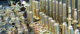
. Copper plating is of great importance in the electrical field. Due to the low cost of copper plating compared to silver or gold plating, coatings are often used for copper plating of electrical busbars, contacts, electrodes and other live elements. Copper plating is often used as a coating for soldering. Also, copper coatings are used in high-load components as a solid lubricant and protection against scuffing, for example, when screwing together threaded connections.
Copper plating is often used to protect areas of steel parts from carburization and nitriding (saturation with carbon and nitrogen). Only those areas that are subsequently subject to cutting processing are coated with copper (hard carburized surface layers do not lend themselves well to such processing, and copper protects the coated areas from the diffusion of carbon and nitrogen into them).
Copper plating of metal is often used in restoration work when restoring chrome-plated parts of automobile or motorcycle equipment, in which a large layer of copper 100-250 microns or more is applied, which closes the pores and defects of the metal, is polished and serves as a new base for applying subsequent coatings.